Platform for creating and sharing projects - OSHWLab


Stars2026


Activity
More
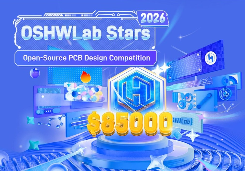
OSHWLab Stars 2026
2025-12-31 ~ 2026-12-31in progress

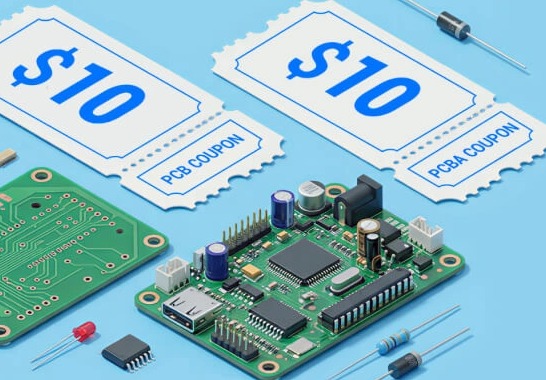
Make Your Own Christmas Gift! 🎁Join · Design · Share · Celebrate🎁 Click to [Get the coupon]
🎄 Christmas Hackathon 2025 🎅
2025-11-12 ~ 2026-01-04activity end

Open to all college and high school students majoring in electronics or enthusiasts. Preference will be given to individuals with experience in campus activities, community building, and student leadership roles.
Campus Ambassador
2024-01-01 ~ 2026-12-31in progress
Collections
More


333 project in total
Enter the Collection >
32 project in total
Enter the Collection >


Forums
MoreSchematic
Need Help With my drone project
Latest Reply:
4 days agoThat’s really nice. You’ve done a great job of partitioning the functionality.
For what will your flight controller be used?
Can your drone develop any special applications which can distinguish it,
To offer it extra leverage into the market?
Would you like any free consultation around attaining a super-potent implementation,
To yield enhanced success in your venture?
We are of course curious about your work, and your vision, ideas, and concepts.
PCB
Is this possible with standard version
Latest Reply:
3 days agoYou can basically buy these modules from any webshop, like Aliexpress, Amazon or Ebay
Then you just find the module footprint and schematic symbol from user contributed library. Then you can solder female headers to your base PCB and attach these modules in them.
Regards,
Markus Virtanen
HW / Electronics Designer
Project
Underwater Vehıcle
Latest Reply:
5 days agoYou are posting an image of BlueRobotics undewater drone, which is already open source. Do you plan to improve it or design a completely new one? Why?
PCB
Experienced electronic engineer but can't find components
Latest Reply:
6 days agoIf the search is not available in easyeda, it can be done on our LCSC: https://www.lcsc.com/products
If the search on the LCSC is not available, it means that we do not have this component.
You can choose to apply for a new component:https://easyeda.com/page/apply-new-part
Featured Articles
More Activity
Materials application instructions
Introduction: Only support "OSHWLab Stars" projects.
The order amount cannot exceed $5,000
2.4k
13
 Technique
Roll the Future: Create Smart Timer Dice
Introduction: Welcome to OSHWLab Weekly: Create, Innovate, Explore. Discover projects and master EasyEDA!
435
4
 Technique
Ordering Boards for OSHWLab Projects
Introduction: Are you new to this hobby, do you want to replicate a community project? Here's the easy way
786
6