

 Completed
Ever Modular V1
License
:CERN Open Hardware License
Description
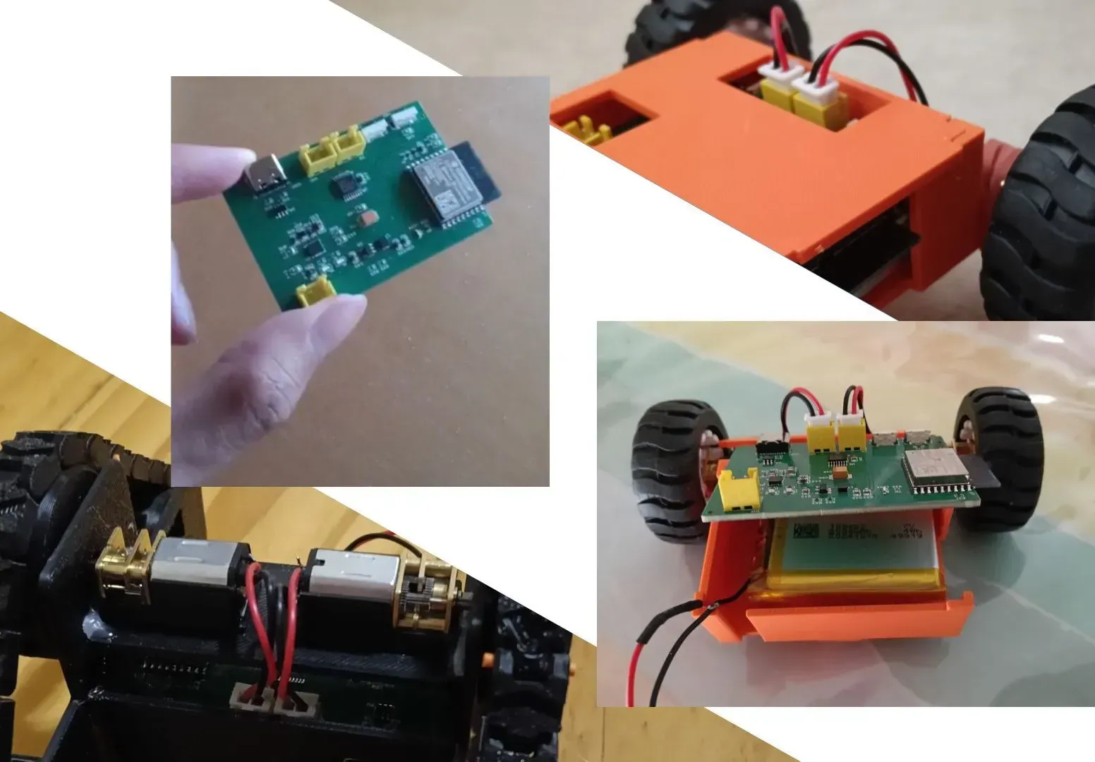
For as long as I can remember, I have been fascinated by the idea of designing and building small RC cars with unique and versatile designs. This project focuses on creating a compact and adaptable PCB specifically for small RC cars. The goal is to make a pcb that can be integrated into various RC car designs, making it both practical and educational for anyone interested in electronics and robotics.
# DEMO VIDEO
Demonstration video for Ever Modular V1
This is my first prototype and will demostrates as a base for my future project!
The PCB incorporates the BQ24074 for efficient battery management, a DRV8833 motor driver to control two DC motors, and an ESP32-C3 microcontroller equipped with boot and reset buttons for convenient programming and operation. Additionally, a buck converter is used to step down VIN/5V to 3.3V, ensuring stable power delivery to the microcontroller and peripherals. This combination of components provides a versatile and educational foundation for exploring RC car electronics, programming, and motor control.
External components needed:
N20 motors x2
Li-ion battery 3.7v x1
TFT display 12 pins x1
Boot button ESP32 c3:
🔌 Strapping pins and boot mode (from the datasheet)
| Boot Mode | GPIO2 | GPIO8 | GPIO9 |
|---|---|---|---|
| SPI Flash Boot | 1 (HIGH) | any | 1 (HIGH) |
| Joint Download Boot | 1 (HIGH) | 1 (HIGH) | 0 (LOW) |
📌 In this table “1” means HIGH, “0” means LOW at reset. documentation.espressif.com
So during Joint Download Boot (the ROM bootloader mode used to flash firmware), the required conditions are:
- GPIO2 is HIGH
- GPIO8 is HIGH
- GPIO9 is LOW ✨
This matches your statement — and exactly what the datasheet shows. documentation.espressif.com
🧠 But what does that really mean in practice?
➤ GPIO9 is the only one you actually need to toggle
GPIO9 is the only strapping pin you actively need to pull LOW when you want the ESP32‑C3 to enter download mode. That’s why dev boards only give you a BOOT button on GPIO9 plus a RESET button. documentation.espressif.com
➤ GPIO2 and GPIO8 don’t need buttons
- They must be HIGH at reset for Joint Download Boot, but:
- Both have internal weak pull‑ups
- You can add external pull‑ups (recommended) so they stay HIGH
- They do not need buttons or switches to pull them low intentionally
The datasheet even says:
GPIO2 actually does not determine SPI Boot and Joint Download Boot mode, but it is recommended to pull this pin up due to glitches. documentation.espressif.com
So GPIO2 is HIGH for both modes anyway; it doesn’t decide the boot type — it just helps keep things stable.
🧠 Why the table says GPIO8 = HIGH for Joint Download Boot
In the datasheet table the download mode line shows GPIO8 as 1 (HIGH) — meaning it must not be pulled LOW at reset if you want reliable download mode. documentation.espressif.com
That’s why many designs add a pull‑up resistor on GPIO8 too — to ensure it’s not inadvertently LOW when you’re trying to enter download mode.
USBC + ESD
- Previous project from: Little Companion Robot | P1.Schematic2 | EasyEDA Pro - V2.2.45
- USB_DP → D+ → IO19
- USB_DN → D− → IO18
Thanks for the feedback and recommendation from the community, I changed from using TVS protection diodes to USB 2.0 protection IC for a stronger protection.
USBC Schematic and Layout Review : r/PrintedCircuitBoard
【ESP32-S3】1.69寸触摸屏迷你控制器~ - 立创开源硬件平台
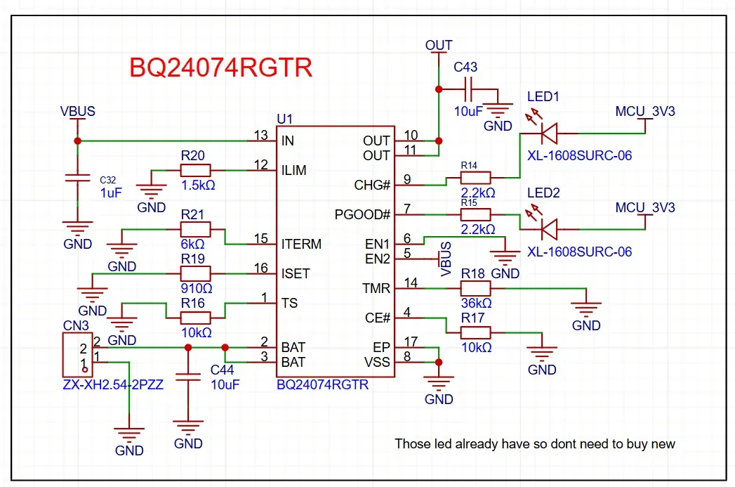
BQ24074
- BQ2407x Standalone 1-Cell 1.5-A Linear Battery Charger with PowerPath datasheet (Rev. N)
- Using BQ24074RGTR
Diode used SS34 for 3.7v battery towards BQ24074RGTR
Pin 13 and 8 is checked and proof.
68532e9eb06c6.png (10079×7128)
BQ2407x Standalone 1-Cell 1.5-A Linear Battery Charger with PowerPath datasheet (Rev. N)
EasyEDA(Standard) - A Simple and Powerful Electronic Circuit Design Tool
CHG and PGOOD (checked and proof)
- CHG - charging status (Whether it is fully charge or not yet)
- PGOOD - weather is good to power up system
- Use led to indicate, connected to 3.3v and resistor
EP, CE#, VSS (checked and proof)
connected to gnd
ISET - Used for setting the maximum battery charging current
- connect a resistor to gnd
- 910 ohms connected → 0.98A charge current
ILIM - limits maximum current drawn from USB / VBUS
- resistor between gnd
- 1.5k ohms connected → 1A current pass through from USB
TMR - sets the maximum charge duration for the battery (Safety timer)
- resistor between gnd
- Connected to 36k to achieve about 3 hours charging time
ITERM - prevent overcharging
- resistor between gnd
- connected 6k resistor for 10% capacity
OUT - main power output
- Voltage follows VBAT when USB is disconnected (battery supplies system)
- When USB is connected, voltage is regulated by the charger (VBUS – charge circuit)
- Voltage follows VBAT when USB is disconnected (battery supplies system)
- When USB is connected, voltage is regulated by the charger (VBUS – charge circuit)
EN1 and EN2
- connect to out is the bets for now for normal charging
- https://chatgpt.com/s/t_694e221f8620819195b2bd24b4f862e9
My Work (Everything is proven) BQ24074
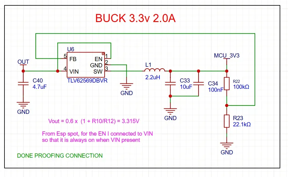
Buck convertor TLV62569DBVR
- Same as previous project
- Used the two resistors to make sure is 3.3v output
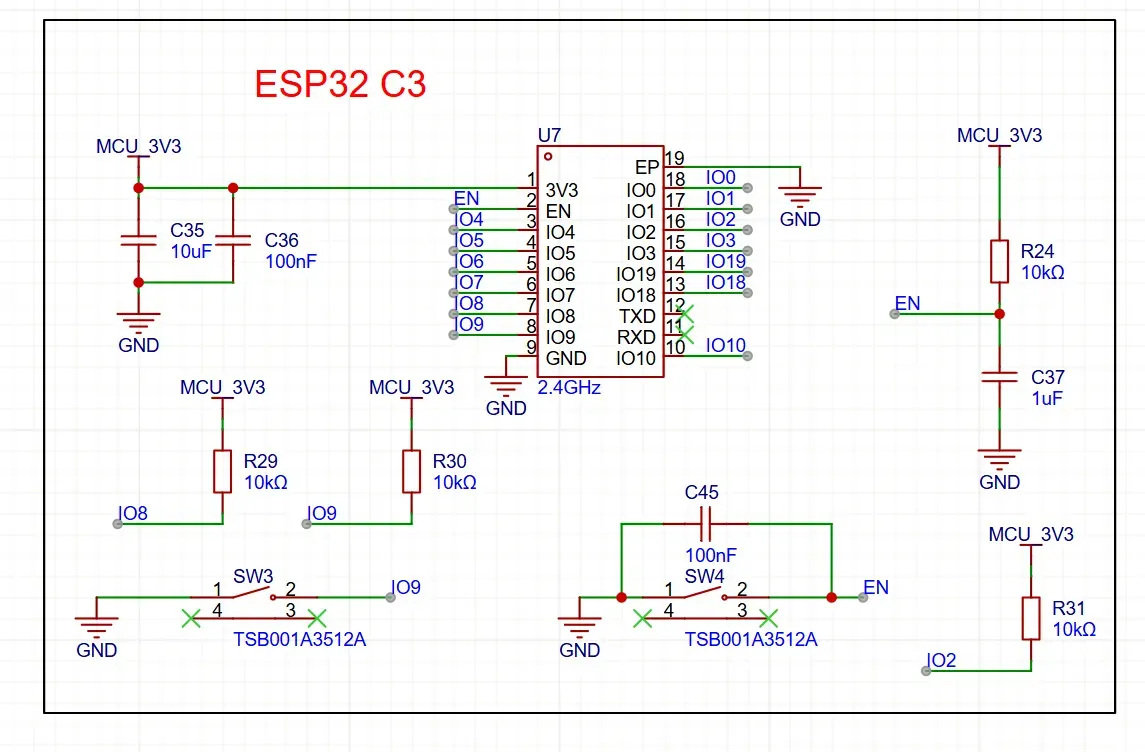
ESP32 c3
ESP32-C3-WROOM-02 N4 chosen
- Cheaper, more gpio, simpler design
- No usb to uart needed just connect directly with gpio 18 and 19 according to datasheet
Espressif Centralized Documentation Platform (CDP) | Espressif Documentation
sch_esp32-c3-devkitm-1_v1_20210
IO9 - Boot
EN - Reset
Explain why EN should connect to the capacitor!
https://chatgpt.com/s/t_694f62087f1c8191b6d8267a706b2037
RGB and LED
- From previous project
- Rgb led used 5v meanwhile led is for checking if buck convertor works properly
Drv8833
- Using drv8833pwr
DRV8833 Dual H-Bridge Motor Driver datasheet (Rev. E)
JLCEDA(Standard) - A Simple and Powerful Electronic Circuit Design Tool
Experiment before continuing:
- Find out which gpio pin to use
- Find out pin for motor
- Find out all pins that required to use
STBY → NSLEEP → 3.3v
NC → Don’t care at all
AISEN and BISEN need to be connected to gnd!
https://chatgpt.com/s/t_6950aadf89e88191bff77e11028a25e6
VCP → connect to VM through 10nF capacitor (By official datasheet and oswhub)
VIN → VIN (3.7v/5v)
AOUT1/2 & BOUT1/2 → Motor output
AIN1/2 & BIN1/2 → GPIO connect
| Function | Pin |
|---|---|
| Motor AIN1 | IO4 |
| Motor AIN2 | IO5 |
| Motor BIN1 | IO7 |
| Motor BIN2 | IO8 |
| RGB LED data | IO2 |
Wazzever Hardware License (Source-Available, Non-Commercial)
Copyright © 2026 Wazzever
This hardware design (including schematics, PCB layout, and related files) is provided for personal, educational, and non-commercial use only.
You are permitted to:
- Study, modify, and build this design for personal or educational purposes
- Share unmodified copies for non-commercial use with proper attribution
You are NOT permitted to sell, distribute, or otherwise monetize this design without prior permission from the author. Permission is free to request; you just need to ask.
- Sell, manufacture for sale, or commercially distribute this design or derivative works without explicit written permission from Wazzever
Attribution: You must credit "Wazzever" as the original designer in any use or redistribution.
Commercial licensing: If you wish to sell, manufacture, or otherwise monetize this design, please contact: junjueang@gmail.com
This design is provided "as is" without warranty of any kind.
Design Drawing
BOM
 Clone
CloneProject Members
Intellectual Property Statement & Reproduction Instructions
This is an open-source hardware project. All intellectual property rights belong to the creator. The project is shared on the platform for learning, communication, and research only; any commercial use is prohibited. If your intellectual property rights are infringed on EasyEDA, please notify us by submitting relevant materials in accordance with the Rules for Complaints and Appeals of IPR Infringement.
Users must independently verify the circuit design and suitability when replicating this project. All risks and consequences are borne by the user, and the platform assumes no liability.
 Empty
Empty
Comment