Editor Version ×
Standard

1.Easy to use and quick to get started

2.The process supports design scales of 300 devices or 1000 pads

3.Supports simple circuit simulation

4.For students, teachers, creators

Profession

1.Brand new interactions and interfaces

2.Smooth support for design sizes of over 5,000 devices or 10,000 pads

3.More rigorous design constraints, more standardized processes

4.For enterprises, more professional users

Completed

PRO MakerLab Small Power Analyzer

Small Power Analyzer

Project tags

License

GPL 3.0

License: GPL 3.0

Mode:

Mode

Editors' pick

Editors' pick

  • 244
  • 0
  • 1
Update time: 2024-08-28 07:57:38
Creation time: 2024-08-27 03:48:10
Description

Description

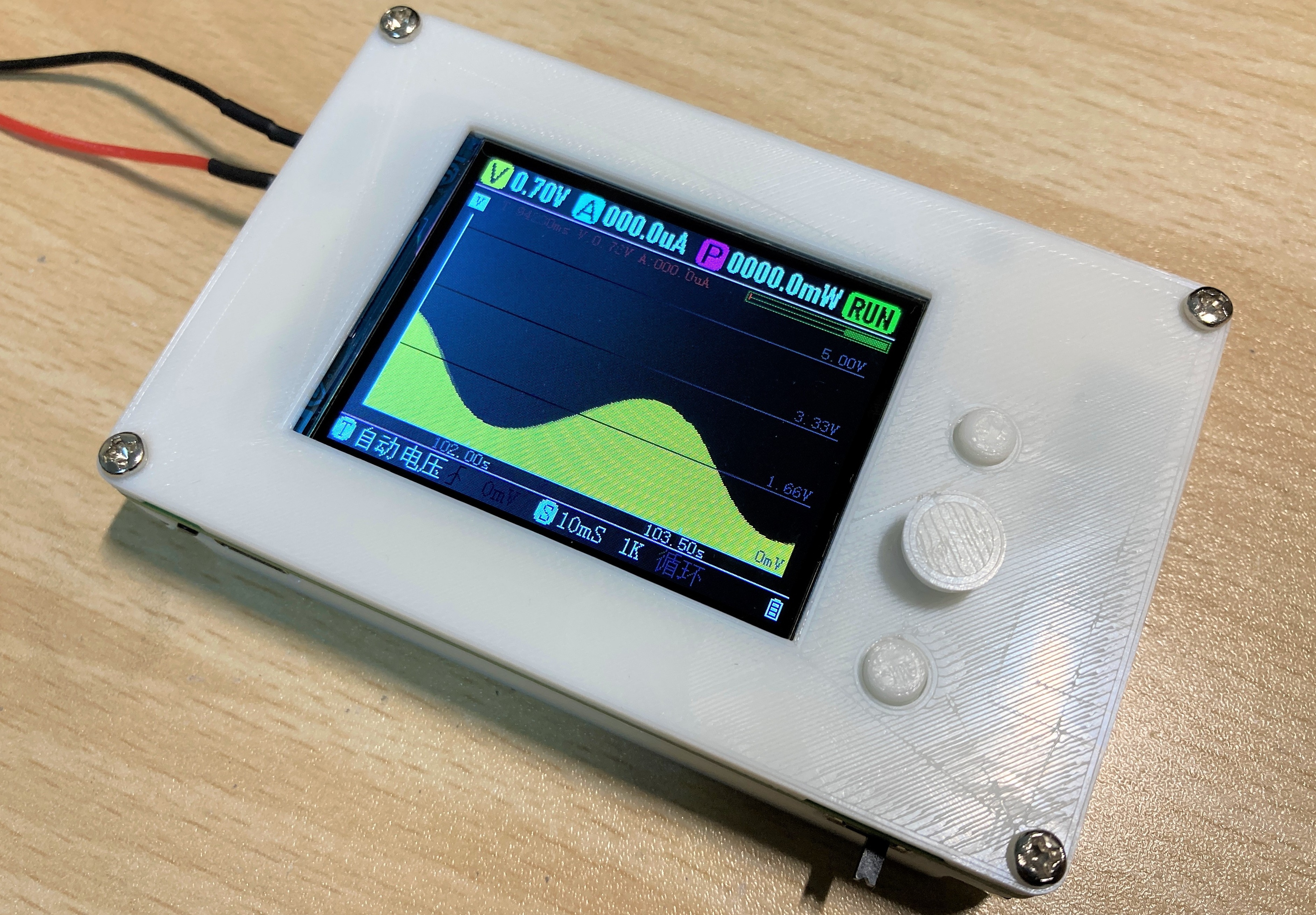
# 1.Project Function Introduction ![image.png](//image.lceda.cn/pullimage/F6bVJavwD7IQwZzVuoOhHKYUfIGp7fLhvqANRF6v.png) Previously, I made a battery-powered low-power mobile device. In order to evaluate the battery life, it is necessary to know the power consumption of the device in a sleep cycle. Because the working current of the device is constantly changing, ordinary multimeters are not competent, so a precision power meter that can measure, record, and analyze current changes is required. However, this instrument is very expensive in professional grade, and it is not cost-effective for a practice project, and it is not convenient to use an oscilloscope and an amplifier circuit. So this project was born. This project is a small portable precision power meter, which can achieve current measurement of up to 1uA. With a 2.4-inch QVGA screen, it can record the current consumption of the device or the voltage change of the power supply, and display it in a graphical way, which is convenient for power supply or power consumption analysis. The fuselage comes with its own battery, which supports complete offline operation, without the need for a host computer. At the same time, it can upload sample data to a PC for more detailed data analytics. Support trigger sampling function, which can easily record occasional events. The sampling rate of up to 100SPS meets the needs of most scenarios. characteristic: * Digital voltmeter and ammeter functions * 2.4-Inch color LCD display * Voltmeter range: 0~ 5.5V, resolution 0.01V, ammeter range: 0~ 1A, resolution 0.1uA (effective value 1uA) * Sampling rate: up to 100SPS, minimum 0.01SPS * Maximum sampling depth 6kpts * Data logging, playback and chart display functions * Support cursor, you can review sample records at any time * Support trigger sampling, working mode: automatic, manual, conditional * Conditional triggering supports voltage and current triggering * Trigger Edge: Rise, Fall * Support data upload (via USB universal serial port protocol) * Built-in 700mA battery, can be used offline for up to 4 hours, charging method: USB TYPE-C * For more feature demonstrations, please refer to the video. The hardware part of this project is 100% designed using Easyeda. The software and hardware of this project are completely open-source, allowing you to browse, download, or develop on this basis. However, unauthorized commercial use is prohibited. # 2.Project Attributes This project is the first to be published and is my original project. The project has never won a prize in any other competition. # 3.Open Source Protocol This project is completely open source, including PC-side host code and MCU-side code. Distributed using the GPL3.0 protocol. # 4.Hardware Part ## Basic working principle The basic working principle of the device is shown in the figure. This project is essentially a packaged voltmeter plus an ammeter, but additional sampling, storage, and processing functions are added to the test results, which can be used to observe the change of voltage or current over time, or to analyze data over a specified period of time. ![image.png](//image.easyeda.com/pullimage/frF6xJ0MdiGRmBlWs8LeFInLI1ZLLZXlFaPUyi55.png) ## PCB Overview ### Back ![image.png](//image.lceda.cn/pullimage/xzXyKaWZBYTOErkTCT1fY6W2FXgHZdERBo8vxAFi.png) ### Front ![image.png](//image.lceda.cn/pullimage/YMRAL3Y8jt6Dntux1o7Xr8q4CzdItHAdJPI06Q0g.png) ## Hardware Architecture The hardware structure of the project is mainly composed of the following components: * Sampling and amplifying circuits * Analog-to-Digital Converter (ADC) * Power Management Module * Input (user keys) and output modules (LCD and USB-UART) * MCU ![image.png](//image.easyeda.com/pullimage/lgVQjJuvs8dLiP3G9rAfrYIOPBK2uIpkIubJGoGt.png) ## Sampling And Amplifying Circuits ### Overview of Current Sampling and Amplifying Circuits #### Schematic ![image.png](//image.lceda.cn/pullimage/BqkvGjonyh5g7Hk1Gg4JDirV6RW2ZO57I7mGsSGH.png) #### PCB ![image.png](//image.lceda.cn/pullimage/5LzvpeppXjVvjnhimutZJPUvcQ9rmbqSXBmqM4xM.png) The sampling of current is the focus of this project. In this project, the sampling resistor low-side current sampling is used to sample the current. Because the maximum current resolution of this project is 0.1uA, and the maximum range of the current is 1A, the difference between the two is 10 million times. If it is realized by a single sampling resistor, then not only the sampling resistor should choose a higher resistance model, but also the operation amplifier needs to be used to amplify the sampling result by more than 1000 times, which may introduce a lot of errors and noise in the measurement results. Therefore, this project uses two sampling resistors with different resistors. Among them, the low resistance (0.1 Ω) resistor is used for sampling when the current is large, and the high resistance (10 Ω) resistor is used for sampling when the current is small. The sampling results on each sampling resistor are amplified by two stages through the operational amplifier, and all the amplification results of each stage are drawn out. In this way, there can be a total of four ranges, and the magnification of each range is within the normal range (the order of 10 to 100 times), which can give full play to the maximum resolution of the ADC within the range of each range. Finally, after adjusting the amplification ratio, the design goal of a minimum resolution of 0.1uA (the minimum effective value is 1uA) and a high measurement range of up to 999mA can be finally achieved on the hardware. ### Range Switching Circuit ![image.png](//image.lceda.cn/pullimage/dprChC9zYUotmXlpK0fX5SMAaPiiIYsVVjczrzjf.png) Because two sampling resistors are used, if the two sampling resistors are always connected to the circuit, the voltage drop on the large resistance sampling resistor will become very considerable when the current is large (there will be a 1V voltage drop at a current of 0.1A), which will bring heat on the one hand, and cause the voltage drop at the output on the other hand, which may affect the normal use of the output device. So in order to solve this problem, this project designs a range switching circuit. When the current is large (the threshold set in this project is 10mA), short-circuit the large resistance sampling resistor through a MOSFET, and then turn off the MOSFET when the current is less than the threshold, and connect the sampling resistor to the circuit. In this way, the problem of voltage drop on the high resistance sampling resistor under high current is perfectly solved. ### Current Amplifier Circuit ![image.png](//image.lceda.cn/pullimage/MPwm7sAvkrq7I2P9A2aDxT2a1ZTkR6TFuqowGtdS.png) The amplification circuit corresponding to each sampling resistor is composed of a two-stage operational amplifier circuit. The primary amplification circuit uses differential amplification to further reduce the error caused by the resistance on the wire, and the two-stage amplification circuit uses a general-purpose positive feedback amplification. For this project, the primary amplification circuit has a magnification of 33 times (10xADC measurement range), and the secondary amplification circuit has a magnification of 9.2 (about 10) times. The amplification results of both stages are introduced into the ADC, plus the two-stage input of another sampling resistor. A total of four stages of amplification results are input to the ADC through four channels. Due to the 100-fold difference in resistance between the two sampling resistors, for the same current signal, the ADC will simultaneously obtain four levels of input (i.e., four gears) for the same signal, so that the ADC can choose the appropriate gear within its own dynamic range as the final output result. ### Voltage Amplifier Circuit Voltage is not the focus of this project, because under normal circumstances, the power supply we have used is a constant voltage power supply, the voltage will not produce a large toggle, and basically there will be no measurement demand for ultra-low voltage (such as less than 1V). Compared with voltage, we are more concerned about the change of current (some similar instruments on the market do not even have the function of voltage measurement, just a simple high-precision galvanometer). Therefore, the voltage measurement range of this project is 0~ 5.5V, and the resolution is 0.01V. ![image.png](//image.lceda.cn/pullimage/iTL6eYR4yGqqA64OreAlBmh4wmC6MDTpwHQQIosa.png) The specific voltage sampling is achieved using a differential amplification (attenuation) circuit, which attenuates the input voltage by 2.13 times, so that when the ADC range is 0 to 3.3V, the maximum allowable voltage input is about 7V, relative to the design goal of 0 to 5.5V, which not only leaves enough margin, but also can give full play to the performance of the ADC to achieve a resolution of 0.01V. ### Op Amp Selection The current signal amplification part uses two high-precision, zero-offset dual-channel R2R operational amplifiers COS8552, which are respectively responsible for amplifying the signal on the two sampling resistors. ![image.png](//image.lceda.cn/pullimage/tLGNSEhhsZ5jVob2axh5NqeksIcTOXUAcJcY1HiT.png) Because the voltage amplification part is not demanding, a general single-channel operational amplifier RS321 is used. ![image.png](//image.lceda.cn/pullimage/9ov8p6RCJjyjrS9CuQYXIuQ6pkwZjIwjEKZxywlP.png) ## ADC From the previous introduction, we can see that the ADC needs at least 5 channels to meet the demand, that is, 4 current channels and one voltage channel. And in order to achieve a sampling rate of 100SPS, the sampling rate of the ADC must also be higher than this design goal. And multi-channel, high-resolution, high-sampling rate ADC is very expensive. Because our requirements for each sampling channel of the ADC are different, we want higher current resolution, but the resolution requirements for voltage are not high, so for optimization, this project chooses to use a separate ADC to sample the current channel, while the voltage and other analog channels (such as battery power and joystick input) are sampled using the ADC built into the MCU. The independent ADC for current sampling finally selected the ADS1115 model, which has a 4-channel 16-bit resolution and uses IIC mode to communicate with the MCU, with a maximum sampling rate of 860SPS, meeting the requirements of this project. ![image.png](//image.lceda.cn/pullimage/x7phMRzlj7jXWxM2patVbBx91z5syIcpm9vi0eRC.png) ## Power Management ### Battery and charge and discharge management In order to be convenient to use and meet the design requirements of completely offline use, this project chose the solution of built-in lithium battery. The charge and discharge management of lithium battery is realized using the classic TP4056, and the design lithium battery capacity is 700mAh, and the size code is 642745 (64mmx27mm length and width, 4.5mm thickness). ![image.png](//image.lceda.cn/pullimage/WoNgRFeHSgMYd0o7qdqcEtfg7av83X6CUd4q5dUh.png) The corresponding battery installation location on the PCB version: ![image.png](//image.lceda.cn/pullimage/xrydVQZYC0ZYJJRy5nuX1vhGaTK5PuHCcvZH2PZC.png) Charge management uses the classic TP4056 charge management IC: ![image.png](//image.lceda.cn/pullimage/74noqzCpPdq5HbDDwqbaUwGvDpP5U5A0hwjs781E.png) The relevant circuits are as follows: ![image.png](//image.lceda.cn/pullimage/9ePCZPRz5LtQN43PI6VW0PrwlvpWMe9YbaOxrZOm.png) ### Power Supply Scheme Because the working current requirement of this project is not large, and it is more sensitive to circuit interference, the LDO scheme is selected for the power supply scheme, and the LDO used is XC6206. ![image.png](//image.lceda.cn/pullimage/cCvHDtFq8HdAK2PUG8Qzr1RXrPtk2x8QtlGmcmAk.png) In order to achieve digital-analog isolation for power supply, plus the backup power required by the RTC part of the MCU, a total of three XC6206 are used to power the digital circuit, the analog circuit and the MCU RTC (backup circuit) respectively. It should be noted that the digital power supply VCC and the analog power supply VCC are turned on by the switch control, while the backup power supply bypasses the switch and is directly connected to the battery. ![image.png](//image.lceda.cn/pullimage/bYtrrPKDcueHCpZzel6xiU4gTKNpcZgy7JfWIBnO.png) ### Battery Level And Charge Detection This part of the circuit is to detect the battery power and charging status, both of which are realized by a resistor divider circuit. In order to reduce the consumption of battery power, the power detection circuit is located behind the switch. The output signals of both are directly connected to the ADC channel of the MCU: ![image.png](//image.lceda.cn/pullimage/lny6CR1wuMZeBcNoWKYvuM1mZlSAYGWwM5vL1XjA.png) ### Analogue And Digital Ground In order to reduce the crosstalk between the analog circuit and the digital circuit, this project uses an analog and digital isolation method, and the two are connected through a single point of 0 Ω resistance: ![image.png](//image.lceda.cn/pullimage/54SCEMpWbooaXLj72EsW093h7EbyJVmuQY8TwnBe.png) ## User Input And Output ### LCD LCD is the main user output channel, and most of the data of this machine is displayed to the user through LCD. After balancing the integrity of the display content, the processing power of the MCU and the project cost, this project chose a 2.4-inch color dot matrix TFT-LCD display with QVGA (320X240) resolution. The LCD communicates with the MCU through the 8bit 8080 bus. After testing, the maximum refresh rate can reach 60Hz. In actual use, in order to reduce the pressure on the MCU, the screen finally works in 8-bit (LUT) color mode and 30Hz refresh rate. The circuit of the LCD is as follows. ![image.png](//image.lceda.cn/pullimage/fQPLThcjrXnEEIDqVJWb922YwtCTpwuw6oAKkyAn.png) The LCD backlight circuit uses a MOSFET controlled by PWM, with a dimming frequency of about 1KHz and a maximum operating current of about 40mA. ![image.png](//image.lceda.cn/pullimage/mZl9Z9aZumuNriyNwjNs6EG4aJdf7qJeEe5vDmfd.png) ### Key The user input for this project is completed entirely by keys, including a five-way switch (joystick) and two touch keys. In order to reduce the consumption of IO and the difficulty of PCB wiring, the joystick uses the connection of the ADC key: ![image.png](//image.lceda.cn/pullimage/wiFBereRbBf45NLJAc3fzmmFn20OrLtJnzB5DDXx.png) The other two keys use independent IO. For possible MCU sleep functions in the future, the run key is triggered at a high level and connected to the MCU's PA0 sleep wake-up IO, and the other option/setting key is triggered at a general low level and connected to the MCU's normal GPIO. ![image.png](//image.lceda.cn/pullimage/uxSjvWakCyMmeHQYXHYGVAY8DfCpVMlZRmIvPe1A.png) ### USB Serial Port In order to realize the upload function of sampling data, a USB-UART bridge circuit is designed in this project, which can upload data to the host computer through the USB serial port. ![image.png](//image.lceda.cn/pullimage/VFvCZ9dZFzaLQqAMD322S9U7yGI7H4YP9wMOfu1o.png) The model selected for the USB serial port IC is CH340E: ![image.png](//image.lceda.cn/pullimage/cdU262RONDZnC9Mj1m3Qrjg3M2bkUgEM4Fb9H8an.png) In this project, the communication parameters of the serial port are 11500 baud rate, 8 data bits, 1 stop bit, and no parity bit. ## MCU The MCU used in this project is STM32F407VE, with 192KB SRAM, a maximum frequency of 168MHz, with ADC and 8080 bus interface, which can meet the requirements of this project for signal sampling and processing and driving LCD. ![image.png](//image.lceda.cn/pullimage/3sX0gtOujdsPsJAOViSt0O9XbPkT92x62LOCczxw.png) # 5.Software Part ## Development Environment This project is developed using the Eclipse-based STM32Cube IDE, and the compiler is GCC. ![image.png](//image.lceda.cn/pullimage/Ijdiz3uokKW38JrObHsHgi7YvVGgSi70EwmpbL9p.png) ## Software Architecture The software architecture of this project is relatively simple. The HAL library is used as the hardware driver of the MCU, and FreeRTOS is used as the software foundation of the whole project. The OS is divided into two threads, one of which is the ADC sampling thread, which is a high-priority thread, and the other is the main thread. The ADC sampling thread is only responsible for sampling the ADC according to a fixed frequency. Other signal processing, user interaction, data display, logic processing, etc. are all completed within the main thread. The graphics processing part uses an 8-bit full-screen framebuffer to reduce the development difficulty and improve the efficiency of screen swiping. The word mode processing part of the graphics library uses part of the LVGL code, and the rest is written by yourself. Screenshot of part of the code of the graphics library used. ![image.png](//image.lceda.cn/pullimage/ufHBBfdqaOTsEXwotzBWmWC6s7t22sOXECoLBaxy.png) The structure of the sampled data is defined using a structure, so that the voltage, current and timestamp data at the time of sampling are saved at each sampling point. The memory consumption of a single data is 8 byte, and a total of 48KB of memory is used to achieve a storage depth of up to 6Kpts. ![image.png](//image.lceda.cn/pullimage/W59IqQHw3Oa2iVnyexaTPPHF4IvCCeWoJgc57jZX.png) # 6.Project Bill of Materials ![image.png](//image.lceda.cn/pullimage/ai46Xcfe9BcIdZ7vclNWxqp6l9Nj9Qq5GPeGCpGr.png) ![image.png](//image.lceda.cn/pullimage/P4EkCDpwhPlvIxnqQ6LeN7aRbjRAsHvN2S2OiVBT.png) # 7.Contest Logo Verification ![image.png](//image.lceda.cn/pullimage/IPz7N20unpnIPYUuGrpMftUbcdPb74G7hSLJyCoU.png) # 8.Other Pictures ## Finished Product Drawing ![image.png](//image.lceda.cn/pullimage/F6bVJavwD7IQwZzVuoOhHKYUfIGp7fLhvqANRF6v.png) ## Front (not turned on) ![image.png](//image.lceda.cn/pullimage/q0UBkhEcksmratf51Z1iJoiAKsGqaDMDADOj4LMH.png) ## PCB back ![image.png](//image.lceda.cn/pullimage/yGoTazAhPi79fI2PnnHp4BwEgKyYQuaI0142BHPk.png)

Designed by micespring (from OSHWHub)

Link:https://oshwhub.com/micespring/handcon

Design Drawing

Design Drawing

schematic diagram
1 /
PCB
1 /
The preview image was not generated, please save it again in the editor.
Empty
Project Members

Project Members

Target complaint
Related Projects
Change a batch
Loading...

Comment

Add to album ×

Loading...

reminder ×

Do you need to add this project to the album?

服务时间

周一至周五 9:00~18:00
  • 0755 - 2382 4495
  • 153 6159 2675

服务时间

周一至周五 9:00~18:00
  • 立创EDA微信号

    easyeda

  • QQ交流群

    664186054

  • 立创EDA公众号

    lceda-cn