

 Completed
Bio-ADDAC
License
:Public Domain
Description
Biosignal : Analog->Digital : Digital->Analog : Convertor
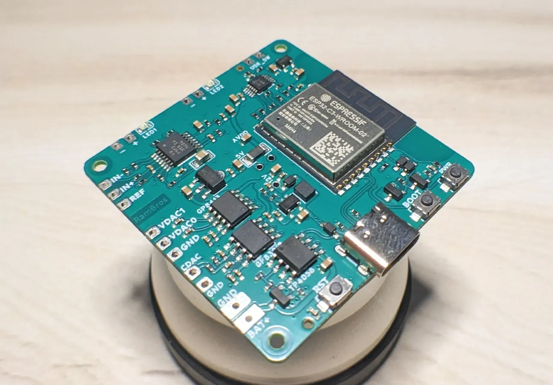
A prototype board to read extremely low amplitude bio electrical signals such as EEG, ECG, EMG. The analog frontend is based on the bioamp EXG board by upsidedown labs.
Additionally this board also has a 15-bit voltage control DAC module and 12-bit current control DAC to produce electrical signals for bio-stimulation.
!!! Be careful when using the stimulation functions, intended for experimental use only !!!
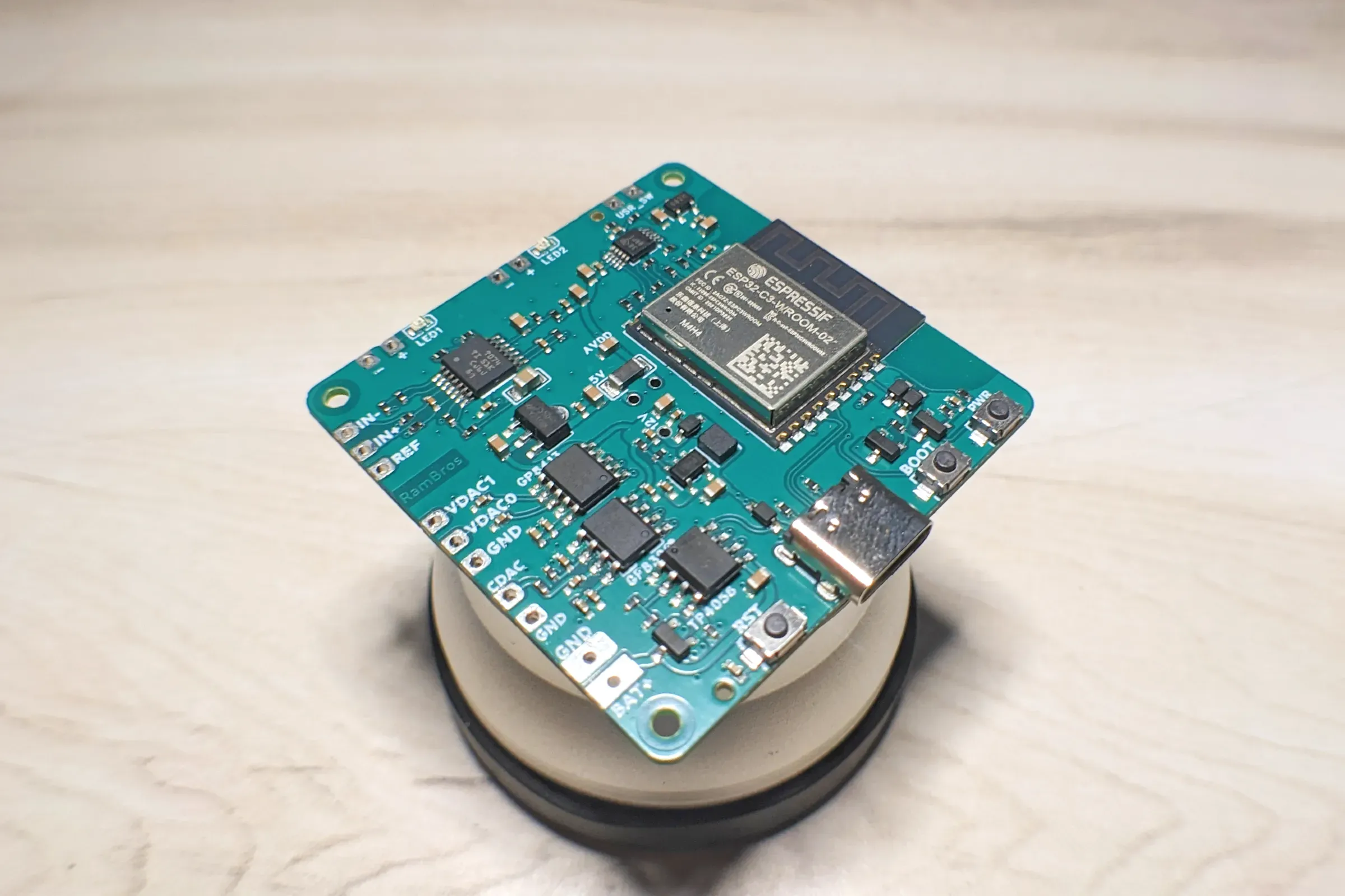
Board Details:
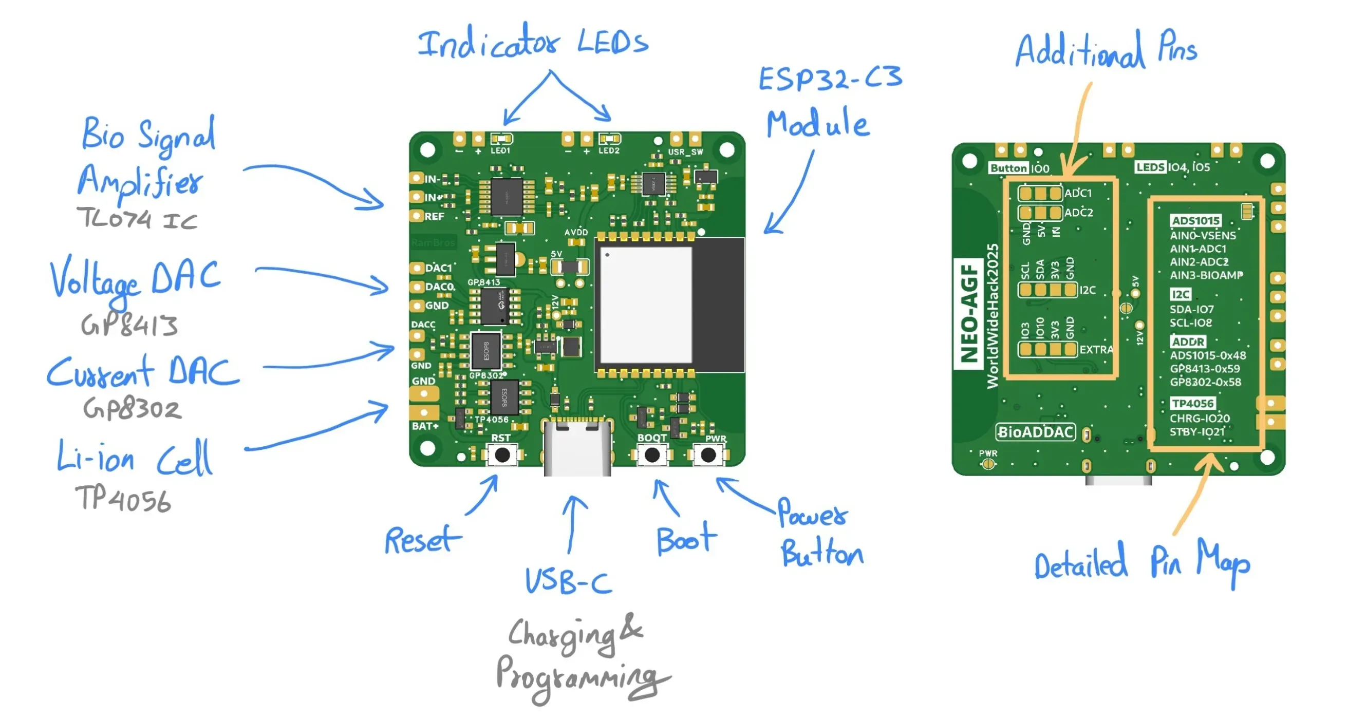
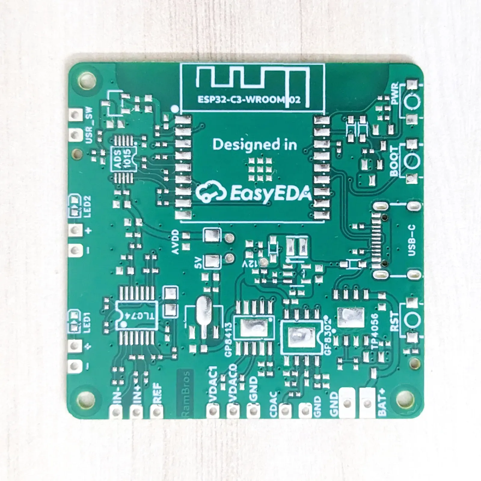
BioAmp:
This is derived from BioAmp EXG Pill, the open source Analog Frontend for measuring biopotential signals. This is based on the TL074 Jfet-input low-noise quad amplifier.
The main difference is how we measure the reading from this; Instead of being directly connected to the MCU's ADC pin, it is connected to the input of the ADS1015 ADC.
ADC:
An I2C (0x48 address) based 12-bit ADC is used for the analog measurements. The main advantage of this approach is the Programmable Gain, it allows us to dynamically adjust the gain depending on the signal type and amplitude. While the 12-bit (0-4096) may seem low, the PGA allows us to maximize the effective resolution for all types of bio signals.
Voltage - DAC:
The GP8413 is voltage control DAC, This can effectively output 0V-10V according to the I2C input (0x59 address).
Caution: As this is a voltage DAC, can easily exceed the 100mA.
Current - DAC:
The GP8302 is a current control DAC (0x58 address). While this can output a range of 0mA to 20mA, for our application - the maximum current is scaled to ~2.3mA for Safety reasons (using 22K RSET).
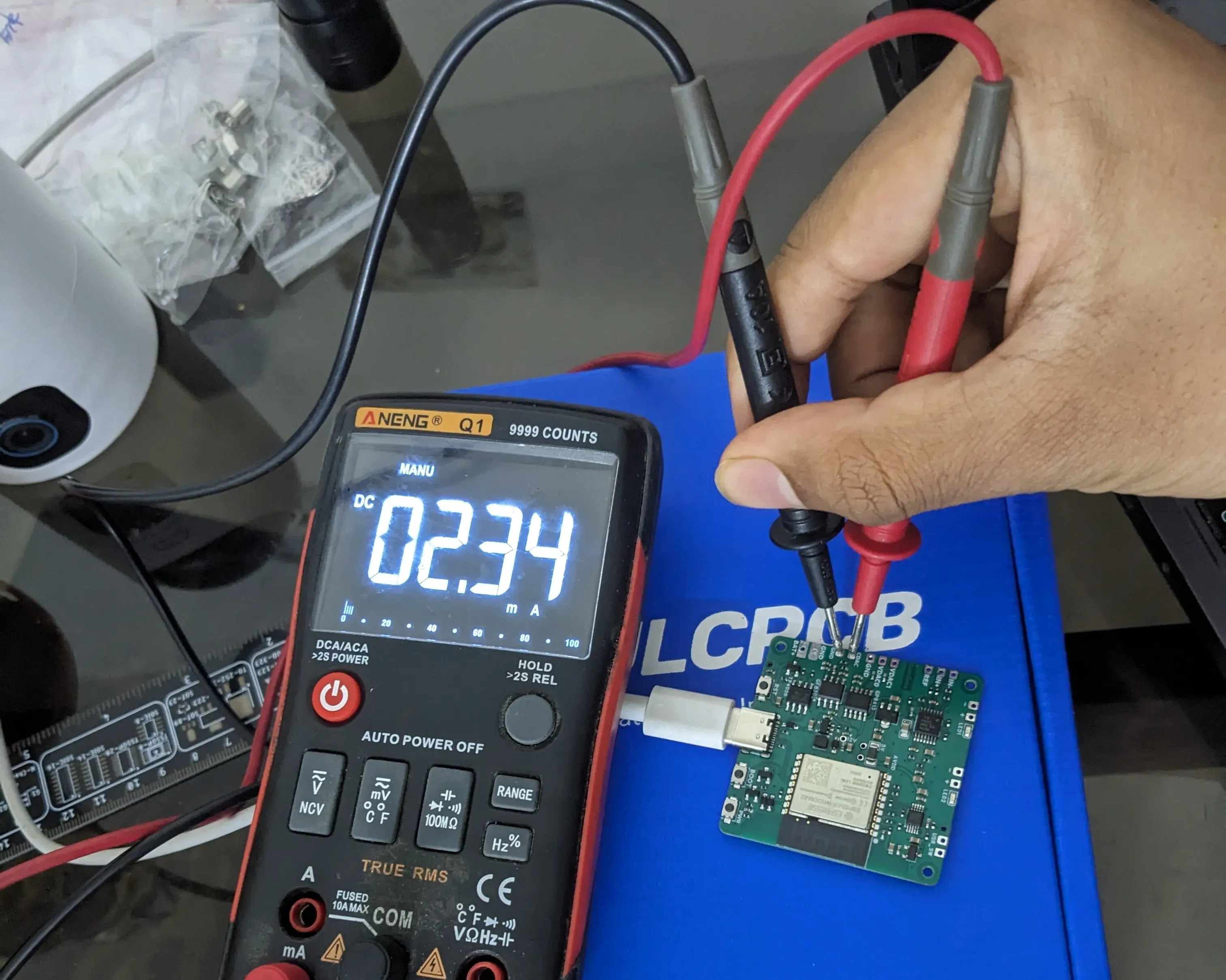
This is the maximum current output ~2.3mA. So it has to be calibrated for this current range (0~2.3mA).
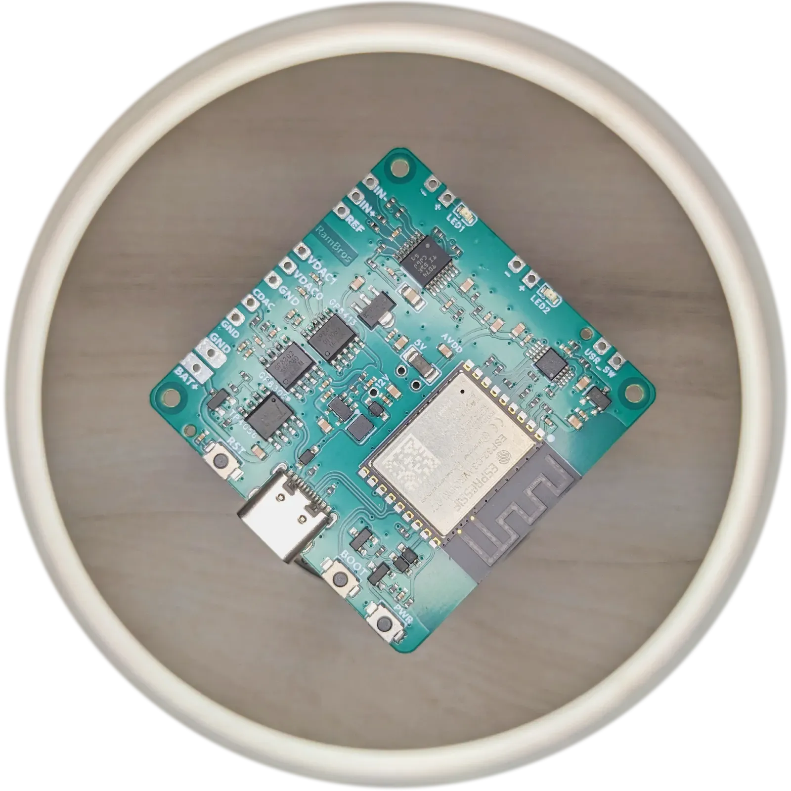
Power Supplies:
- 3.3V LDO - Powers the ESP32-C3 module
- 5V LDO - Powers the ADS1015 and the Bio Amp
- 12V Boost convertor - Power the GP8413 DAC, GP8302 DAC and also the 5V LDO
- Li-ion Cell - This powers the 3.3V LDO and 12V Boost convertor
Power Control:
The board can be powered on by pressing the PWR Button. To keep the board powered ON, the PWR_EN has to be set HIGH - this latches the power mosfet to ON state.
To power off the board, the PWR_EN can be set to LOW.
Note: The power button presses can also be detected even when the board is in ON state.
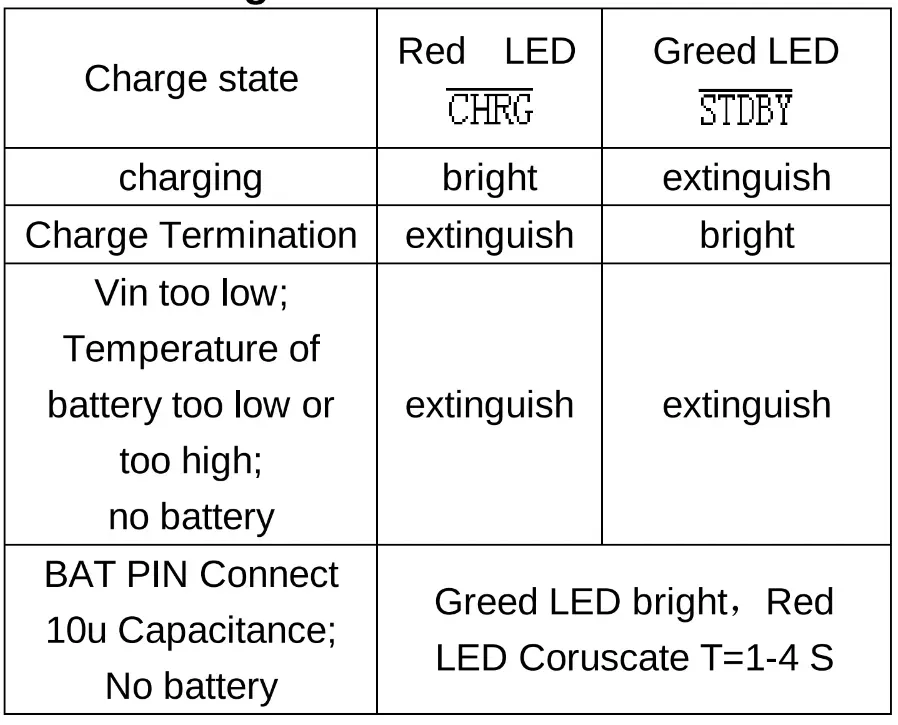
Battery Charging:
The TP4056 is used for lithium cell charging control. The charging current is set to ~500mA
The CHRG and STBY are open drain outputs - they are connected to the MCU for detecting charging state.
Board wiring:
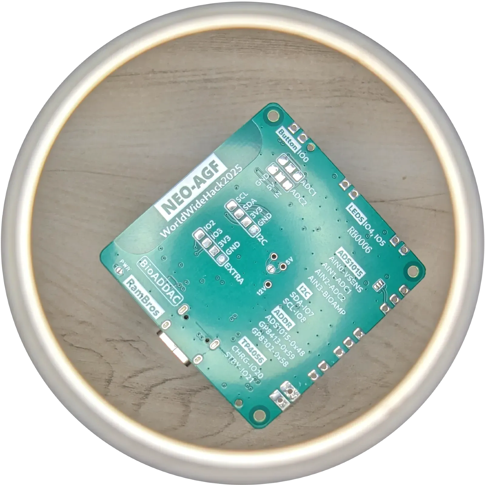
ESP32-C3 pin mapping:
| Function | Pin | Notes |
| PWR_EN | IO0 | set this HIGH to keep the device powered ON |
| PWR_BTN | IO1 | also used as a User button, (INPUT_PULLUP) |
| TP4056_STBY | IO21 | refer table below, (INPUT_PULLUP) |
| TP4056_CHRG | IO20 | refer table below, (INPUT_PULLUP) |
| LED1 | IO5 | Indicator LED |
| LED2 | IO4 | Indicator LED |
| I2C_SDA | IO7 | pulled up to 3.3V with 5.1K resistor |
| I2C_SCL | IO8 | pulled up to 3.3V with 5.1K resistor |
| ADS1015_ALERT | IO6 | can be used for ADS1015 comparator alerts if required |
| GP8302_ALARM | IO10 | Pulled LOW when circuit is open, (INPUT_PULLUP) |
The I2C bus is shared among these ICs with different Addresses:
- 0x48 - ADS1015 ADC
- 0x59 - GP8413 DAC
- 0X58 - GP8302 DAC
ADS1015 pin mapping:
This is a 12 bit ADC with Programmable Gain Amplification, it has a total of 4 channels
| Input | Function | Notes |
| AIN0 | Voltage sense | Read Battery voltage with a voltage divider (R1=220K, R2=22K) |
| AIN3 | BioAmp | Read amplified signals from the bio amp |
| AIN1 | ADC1 | Exposed on the underside of the board |
| AIN2 | ADC2 | Exposed on the underside of the board |
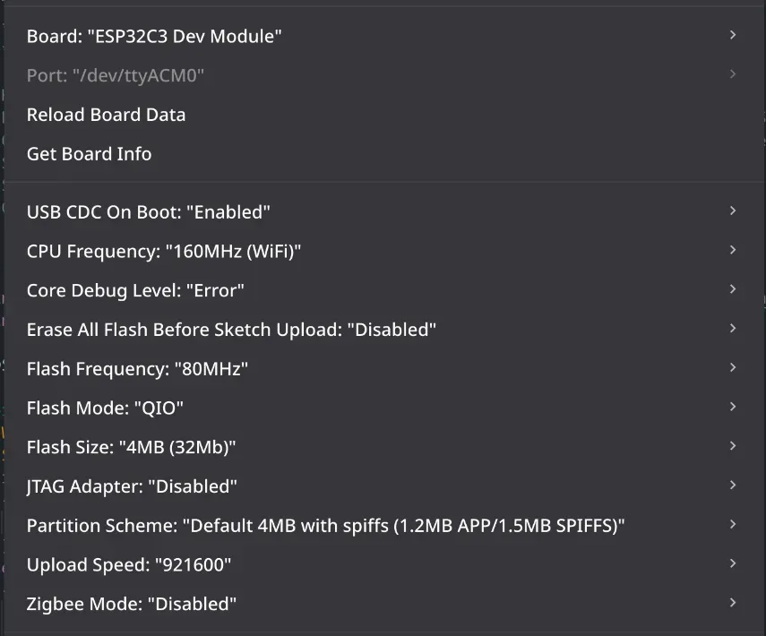
Arduino Compatibility:
The board can be flashed using the ESP32C3 Dev Module definition.
Check I2C devices:
To test the I2C communication, you can use the I2C scanner code - Available here
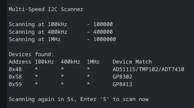
The GP8413 and GP8302 are rated only for 400khz speed, Interestingly these devices respond at 1Mhz speed also.
Tested Libraries:
- ADS1015 ADC - Sparkfun library
- GP8302 Current DAC - Dfrobot library
- GP8413 Voltage DAC - Dfrobot library
Flashing code for the first time:
- Insert USB while pressing BOOT button to enter upload mode.
- Upload the code.
- Press RESET, now the code will run.
This is a one time process, the subsequent uploads are automatic.
Project Origins:
Two weeks ago, a post popped up in my feed. It was about a hardware hackathon called WorldWideHack2025 organized by WorldwideStudios, I found this interesting since most hackathons are usually coding based.
I attended the first meeting and was invited to the NEO-AGF team, and here we are.
- We decided the hardware specs on July 20, the design was ready July 23 and order was placed on JLCPCB rightaway.
- We received the boards by August 1, thats less than 10 days! Do you know any other manufacturer who can fabricate it and get it shipped that fast!

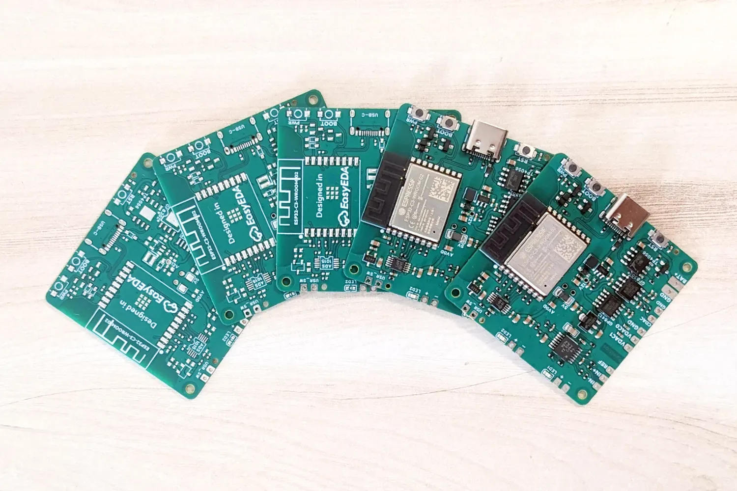
- This project's PCB and PCBA service was sponsored by the OSHWLAB Stars campaign.
- Project was completed on August 2025
Videos from the Team:
EEG signals classification and Stimulation (tDCS) test
Design Drawing
BOM
 Clone
CloneProject Members
 Empty
Empty
Comment