

 Completed
12to5v
STD12to5v
License
:GPL 3.0
Description
Objective:
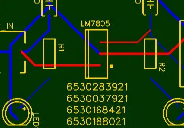
Design and develop a Printed Circuit Board (PCB) system that efficiently converts a 12V DC input voltage to a stable 5V DC output. This system will be used to power various low-voltage electronic components and devices.
Scope:
The project encompasses the entire design process from conceptualization to the final working prototype. The key components of the project include selecting suitable voltage regulation components, designing the PCB layout, fabricating the PCB, and performing rigorous testing to ensure reliability and efficiency.
Key Components:
-
Voltage Regulator IC: Selection of an appropriate DC-DC buck converter or linear regulator to efficiently step down the voltage.
-
Input and Output Capacitors: To filter out voltage spikes and ensure a smooth output.
-
Inductor (if using a buck converter): Necessary for energy storage in a switching regulator.
-
Heat Sink (if needed): To dissipate heat generated by the voltage regulator IC.
-
Connectors: For input (12V) and output (5V) connections.
-
PCB Material: Selection of appropriate substrate material and PCB layout design considerations.
Design Specifications:
-
Input Voltage: 12V DC
-
Output Voltage: 5V DC
-
Output Current: Up to 2A (can be adjusted based on design requirements)
-
Efficiency: Target above 90% for switching regulators
-
Size: Compact design to fit in small enclosures
-
Protection Features: Overcurrent protection, thermal shutdown, and short-circuit protection
Design Process:
-
Requirement Analysis: Define the specifications and requirements of the voltage regulator system.
-
Component Selection: Choose the best-suited voltage regulator IC and other passive components based on the requirements.
-
Schematic Design: Create a detailed circuit diagram using PCB design software.
-
PCB Layout: Design the PCB layout ensuring minimal noise and maximum efficiency.
-
Simulation and Validation: Simulate the circuit using software tools to validate the design before fabrication.
-
PCB Fabrication: Fabricate the PCB using a reliable manufacturer.
-
Assembly and Testing: Assemble the components on the PCB and conduct thorough testing to verify performance against specifications.
-
Optimization: Make necessary adjustments to optimize performance and reliability.
Outcome:
The completed PCB system will provide a stable 5V output from a 12V input, with high efficiency and reliability. This voltage regulator can be used in various applications, including powering microcontrollers, sensors, and other low-voltage electronic devices.
Design Drawing
BOM
 Clone
CloneProject Members
 Empty
Empty
Comment