

 Ongoing
USB Module (3.0 Hub)
PROUSB Module (3.0 Hub)
License
:Public Domain
Description
1. Project Information:
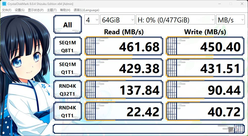
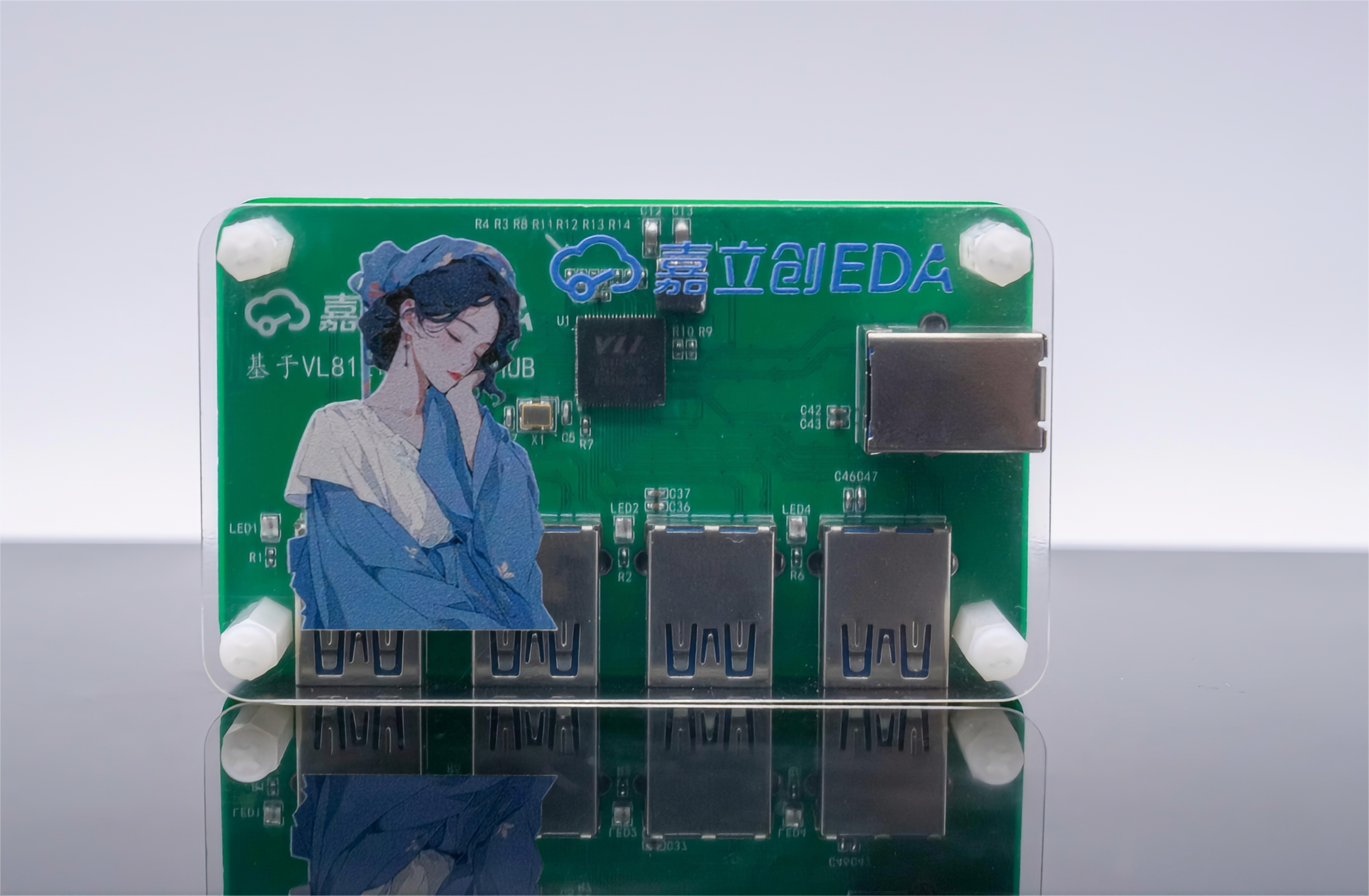
Based on the VL812 USB3.0 Hub, a USB3.0 input, 4-way USB3.0 output, single-supply 5V power supply, the internal integration of 5V to 3.3V, 5V to 1.2V circuit. Self-firmware, soldered and ready to use. Use TYPE-B input interface, easy to weld alignment, measured maximum speed of 461MB/s.
2. Chip Introduction -VL812
- SuperSpeed USB Hub Controller
- Supports four modes: SuperSpeed, HighSpeed, FullSpeed, and LowSpeed
- Four downstream ports and one upstream port
- Integrated voltage regulator to generate all required chip power from 5V inputs
- Supports dual status indicators
- Comprehensive USB battery charging support
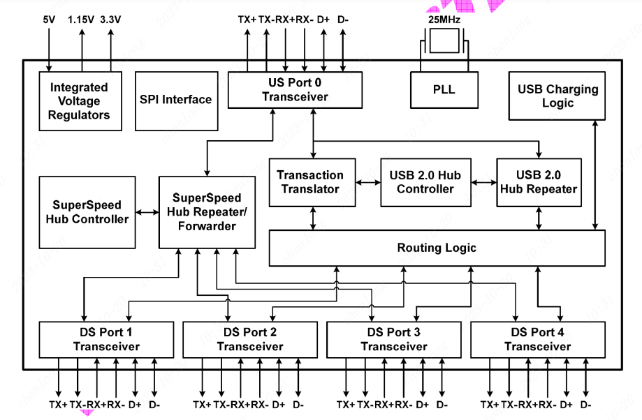
pic-structure diagram
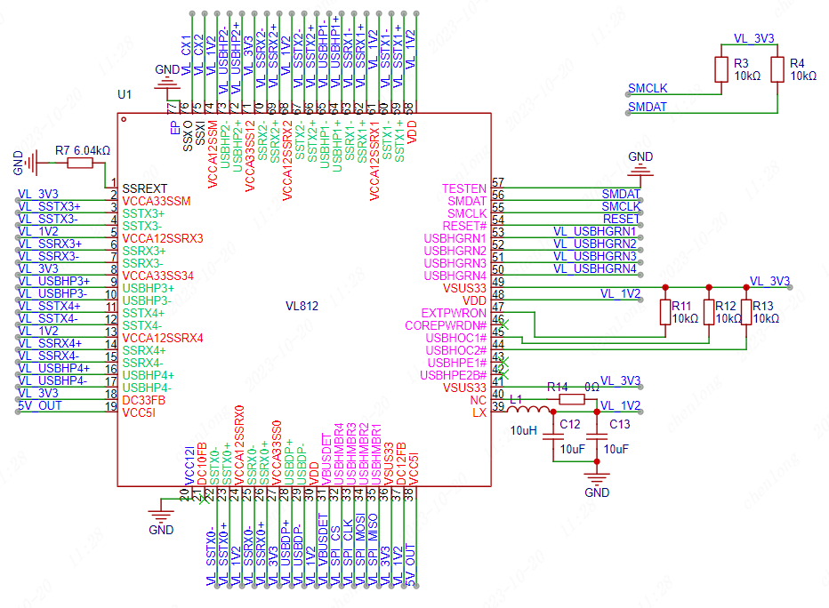
3. circuit analysis

pic-SCH
Control chip circuit
Edit the VL812 chip symbols to distinguish three parts: power supply pin, Hub function pin, and special function pin. Some pull-up and pull-down resistors as well as the LC filtering of the LX pin are not mentioned in the chip datasheet, so it is necessary to refer to the official chip design cases for design.
pic-USB3.0HUB Chip
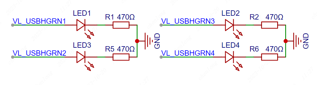
Port indicator light
According to the datasheet instructions, when a device is inserted, the corresponding insertion pin outputs a high level, which corresponds to the addition of an indicator light and a current limiting resistor as an insertion indication. In order to increase the display effect, the indicator here uses RGB3 three-color gradient, internal self RC, without external control.
pic-Port indicator light
Port indicator light
VL812 is a low-level reset, here use 10K resistor with 100nf capacitor for power-on reset to meet the timing requirements. Use 4.7K and 10K to form a voltage divider circuit to divide the 5V voltage to about 3.4V, note that you can't directly input 5V to the pin, it may damage the chip.
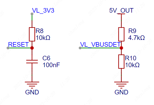
pic-Reset & input detect circuit
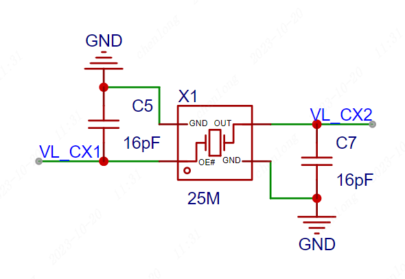
4. Oscillator Circuit
The use of 25M passive crystal to provide a stable clock signal for the main control chip, matching capacitance needs to be based on the purchase of crystal load capacitance selection, you can also consider the use of active crystal to further enhance the stability.
PIC-Oscillator Circuit
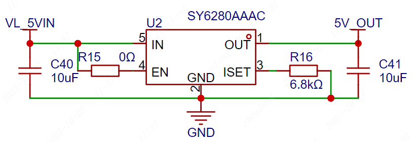
5. current-limiting protection
Considering that some users use notebooks for use, notebook 3.0 interface general output current in 1A or so, here using SY6280 current-limiting protection chip will be the input current now in 1A, to prevent the emergence of burn notebook interface, but if it is the four USB output interfaces are connected to the USB3.0, there may be a lack of power supply, then you need to take into account the actual computer situation is better! Current limiting set resistor R16 for greater current. EN pin direct input can be, high level normal operation, here 0 ohm resistor for the test resistor.
pic- current-limiting protection
6. Input port circuit
USB3.0 protocol and 2.0 protocol is not the same, USB3.0 interface more than one set of differential data input signals, commonly used TYPE-C and TYPE-B interfaces to match these two protocols on the docking interface to make certain changes. Among them, the TYPE-C interface only 24Pin to have differential data lines, can not be distinguished simply by color, we must pay attention when buying!!!!
pic-USB2.0-TYPE-C port
pic- USB3.0-TYPE-C port
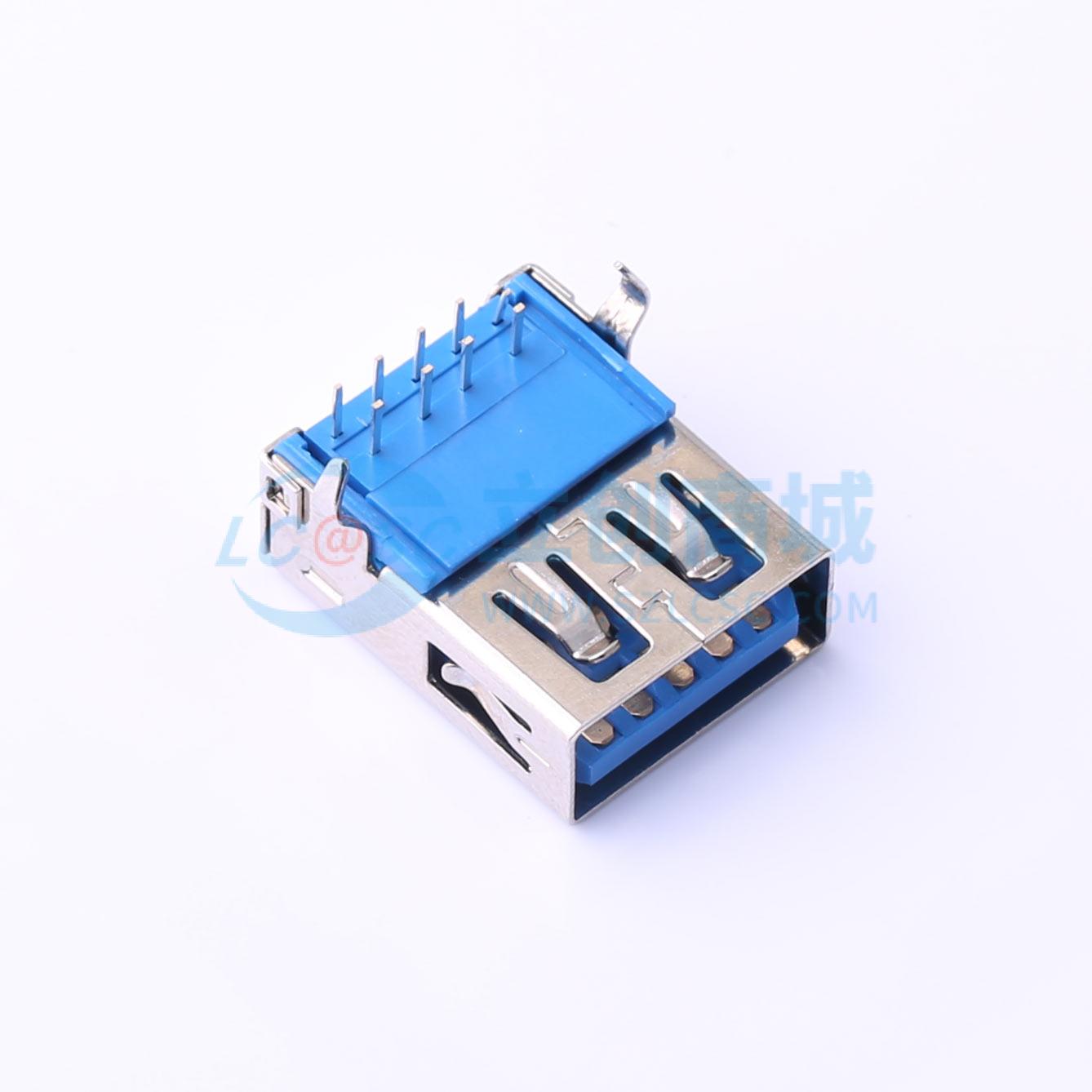
TYPE-B interface in the 2.0 protocol and 3.0 protocol change is very obvious, generally can not buy the wrong, while soldering and alignment is relatively more convenient. This design uses USB3.0 TYPEB interface.
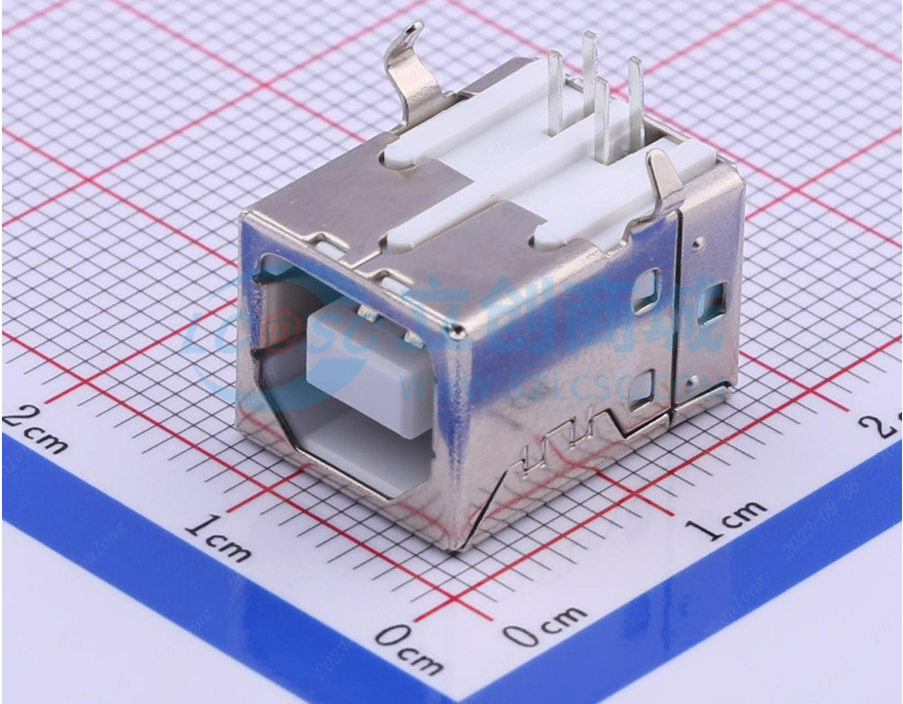
pic-USB2.0-TYPE-B port
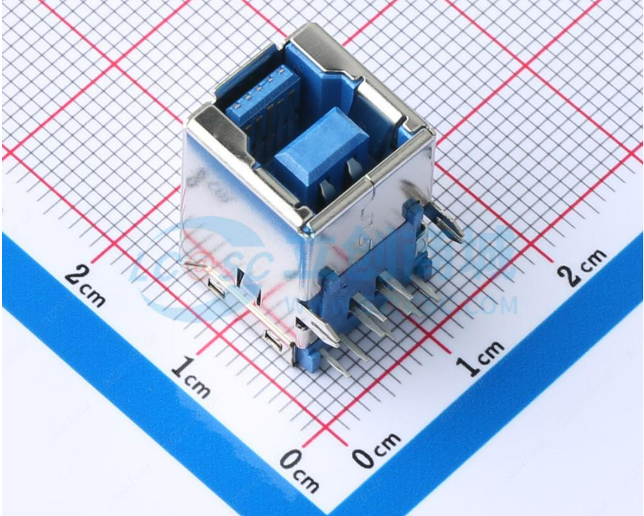
pic- USB3.0-TYPE-B port
In the input interface circuit, the corresponding pin for the lead, in order to better anti-interference effect, generally in the USB3.0 send differential data lines in series with 100nf capacitors for filtering, at the same time, to prevent electrostatic damage to the chip and inserted into the device, in the input part of the addition of TVS tubes for protection.
pic-input port circuit
outpt port
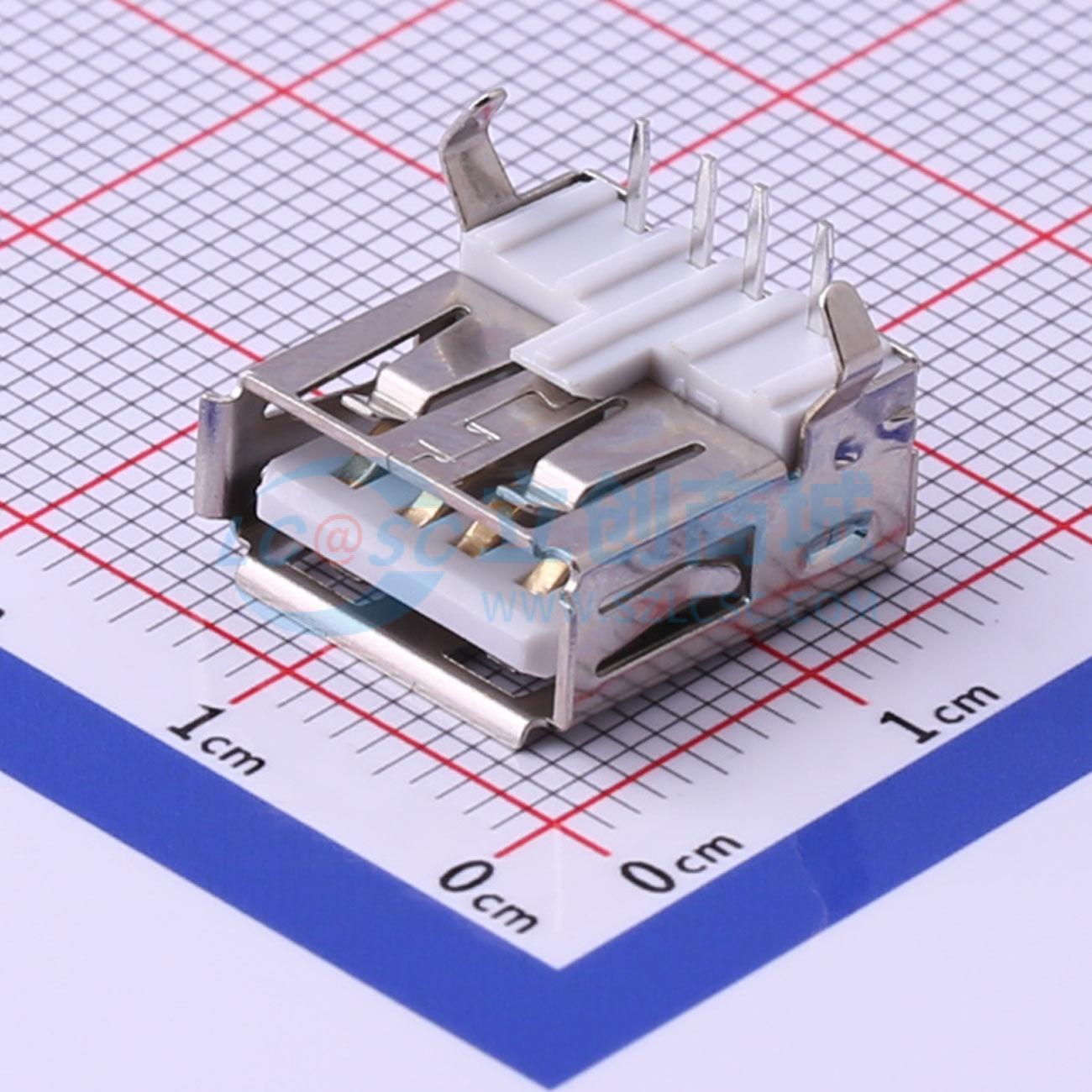
The use of TYPE-A female chassis to expand the output, it should be noted that the TYPE-A interface also has a USB2.0 protocol and USB3.0 protocol points, we need to pay attention to the device selection, it is best to judge according to the corresponding device manuals, the TYPE-A female chassis 2.0 interface is generally 4 pins, 3.0 interface is generally 9 pins!
pic-USB2.0-TYPE-A port
pic- USB3.0-TYPE-A port
After selecting the corresponding devices according to demand, the same plus filter capacitors and TVS tubes for protection, the chip has four outputs, you can first draw all the way, followed by copying the remaining three can be.

PIC- USB3.0 output port circuit
4. PCB Design
1. PCB Layout
- USB interface should be placed close to the board edge or structural positioning, easy to plug and swap;
- TVS tube should be close to the USB interface, it is recommended that the power line out into the TVS tube, play a protective role;
- During layout, consider the distance between the chip and the interface, not too far away, shorten the differential line distance;
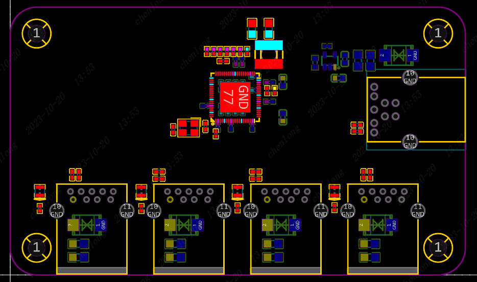
PIC- PCB Layout
2. PCB Wiring
- USB signal to go differential line, impedance control for 90 ohms, and do pack ground out, high-speed differential line length is best not to exceed 1800mil;
- In the alignment, give priority to high-speed differential signal line, as far as possible, do not change the layer, in the layer change, join the return ground over the via;
- Differential pair length error as small as possible, it is recommended that within 5mil
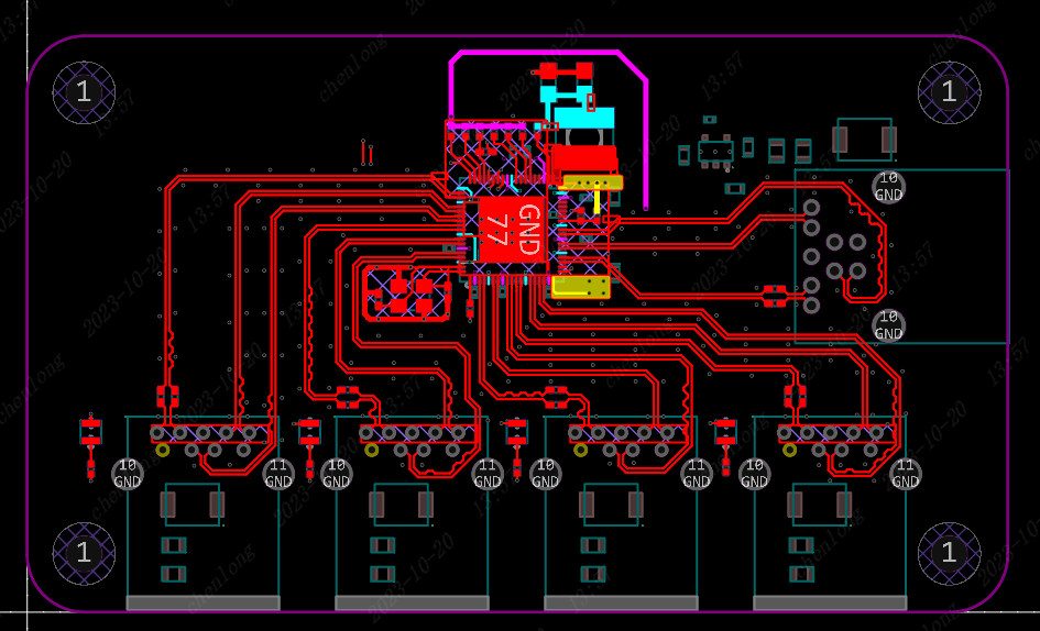
pic- Top Layer
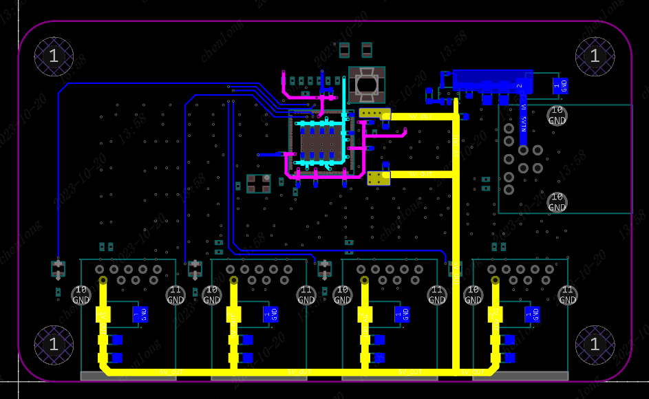
Pic-Buttom layer
Design Optimization
- Prohibited deletion of isolated copper skins;
- Appropriate ground wrapping;
- Adding lifting silkscreen, silkscreen size recommended above 40 mil;
- Adding EasyEDA silkscreen in the appropriate area to designate the location of the guest editor, the finished product is beautiful;
Notes
- Impedance calculation can be found in the Jialitron official website impedance calculation gadget for calculation;
- Power supply alignment needs to take into account the actual current size, this project is limited to 1A, the subsequent increase in current, you need to increase the power supply alignment;
- Welding is recommended to use a wind gun or heating table to weld the main control chip first, and use a multimeter to check whether there is a false weld or short circuit after the welding is completed;
Producet Demo & Testing
Design Drawing
BOM
 Clone
CloneProject Members
Intellectual Property Statement & Reproduction Instructions
This is an open-source hardware project. All intellectual property rights belong to the creator. The project is shared on the platform for learning, communication, and research only; any commercial use is prohibited. If your intellectual property rights are infringed on EasyEDA, please notify us by submitting relevant materials in accordance with the Rules for Complaints and Appeals of IPR Infringement.
Users must independently verify the circuit design and suitability when replicating this project. All risks and consequences are borne by the user, and the platform assumes no liability.
 Empty
Empty
Comment