

 Ongoing
Scanning Tunneling Microscope OpenSTM
PROScanning Tunneling Microscope OpenSTM
8.2k
0
0
0
Mode:Full
License
:Public Domain
Creation time:2023-08-31 01:56:06Update time:2025-04-03 06:37:24
Description
Copyright belongs to @Dimsmary
Introduction
Hi, this project is a project aimed at building an atomic-scale scanning tunneling microscope through DIY.
In June 2022, the project successfully measured the tunneling distance-current curve, the bias-current curve of pyrolytic graphite (HOPG), and the sample size-free qualitative imaging.
In May 2023, the project successfully scanned the carbon atoms of pyrolytic graphite (HOPG).
the branch
This warehouse (due to the size limit of the attachment, please move to GitHub or Gitee for document download) currently creates two branches, namely the main branch (main) and the document branch (Ref-Document). Engineering design files such as source code are placed in the main branch, and documentation materials referenced during the development process are placed in the document branch. The reason why these two parts are separated is because the file size of the document is too large.
Open source file (attachment) structure introduction
- 3D Models
Including shell design files and STEP files required for CNC machining.
- Docs
Documentation in this directory includes project briefs and microscope construction instructions.
- Hardware
Including the single-chip program project file (using Platform IO) written by ESP32 IDF, and the corresponding firmware.
- PCB
The PCB file drawn by Jiali Chuang EDA needs to be opened by Jiali Chuang EDA Professional Edition. Or directly browse online on OSHW-Hub (see the circuit section for details), move to OSHWHUB, and click "Open with Editor" on the upper right.
- PythonScript
For the host computer program of the microscope, please refer to the Microscope Construction Guide for specific usage methods.
Develop technical documents
The technical documentation is still being written and is expected to be released in PDF form, and the old documentation can be downloaded in the attachment.
Version-Release Naming Rules
As of 2022/07, two STM schemes with different mechanical structures have been announced
Although the current STM construction plan is still being revised and improved, the currently released data set can be run to a certain extent, so this project will refer to the way of software release. After the STM plan is updated, the release method will be used to release the plan, the naming rules of the STM solution version number for each release are as follows:
The version number is named after A.B.C. When the mechanical structure of the scheme is refactored, A will change. When the circuit, software, and mechanical structure of the scheme are greatly modified, B will change. C will change when there are minor modifications to the scheme.
Taking 1.0.0 as an example, this version number represents the STM design scheme of the first-generation mechanical structure.
Published version of STM scheme
Release OpenSTM v1.0.0
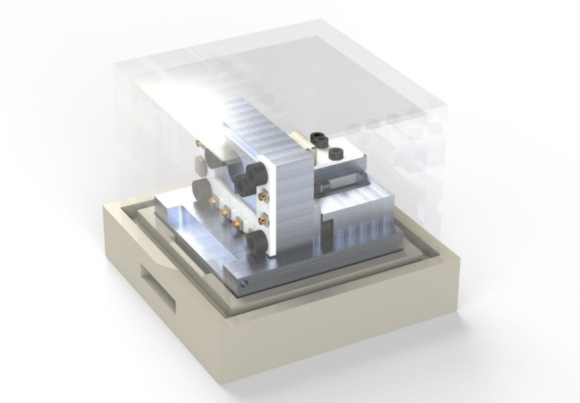
This is the first-generation STM solution. The mechanical structure is built with two aluminum plates:
The scheme is relatively simple, and no experimental results that can be used for analysis have been obtained. However, the construction of subsequent schemes is based on the construction of this first-generation scheme. This version of the scheme is for reference only, and detailed documentation is not provided for the time being.
The published program documents include:
- 3D model file (SolidWorks)
- Arduino program: ESP32 microcontroller control program used to control STM (using LVGL for interaction), vibration detection program based on MPU9250, all developed using Arduino+Platform IO
- PCB and schematic diagram
- Python script for measuring interference fringes
- LTSpice simulation file for power chip
Release OpenSTM v2.0.0
This version plan is the second-generation microscope structure:
The program is structured to measure:
- Tunneling distance-current curve
- Scanning Tunneling Spectrum (STS)
The files included in v2.0.0.zip include:
- 3DModel: 3D model file drawn by SolidWorks, STEP file required for CNC processing
- PCB: schematic diagram and PCB file drawn by EasyEDA Professional Edition
- Software: Under the Arduino folder, it contains the control program of the ESP32 single-chip microcomputer and the control program of the ATMEGA 328P single-chip microcomputer. Under the Python folder, it contains the host computer control software and image conversion program
achievement
Tunneling distance-current curve
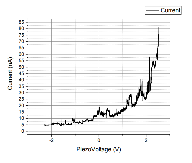 Tunneling distance-tunneling current relationship curve
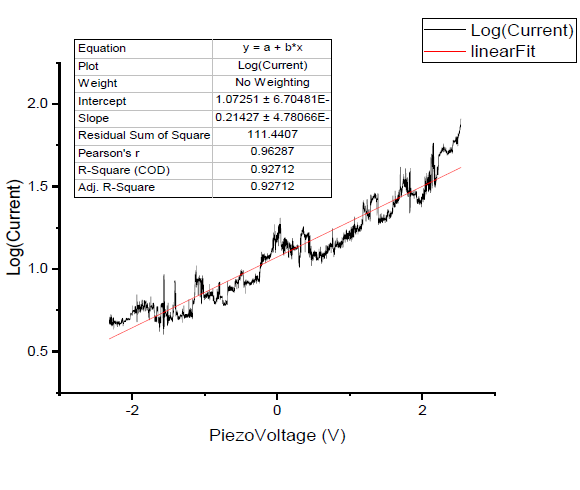 Fitting curve after taking a Log of tunneling current
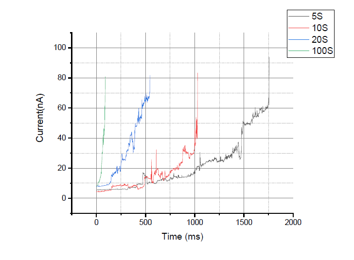 Tunneling distance-tunneling current relationship curve at different approach speeds (bias 50mV)
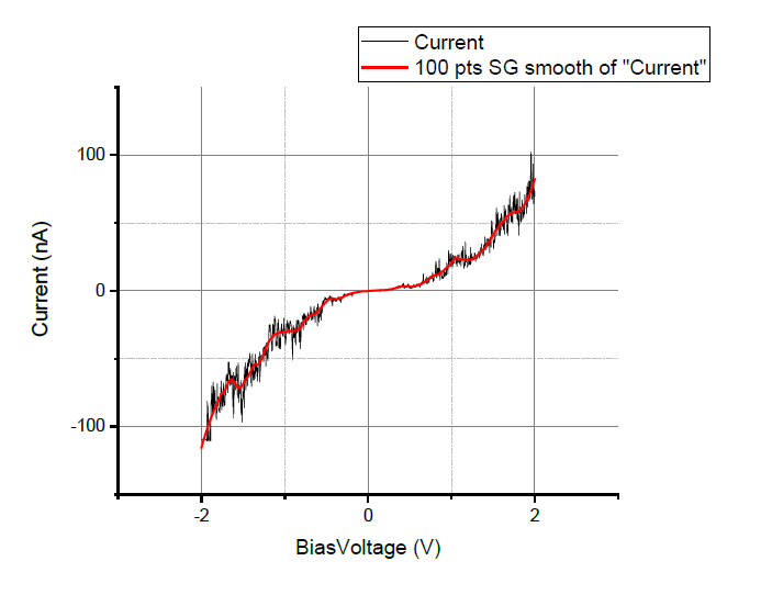
Bias voltage-current curve of pyrolytic graphite (HOPG)
Size-Free Qualitative Imaging of Pyrolytic Graphite (HOPG) Samples
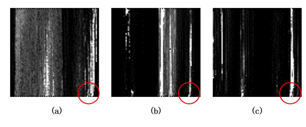 Repeatability test image scanning results (bias voltage 500mV, step size 18.5mV, sampling points 80*80)
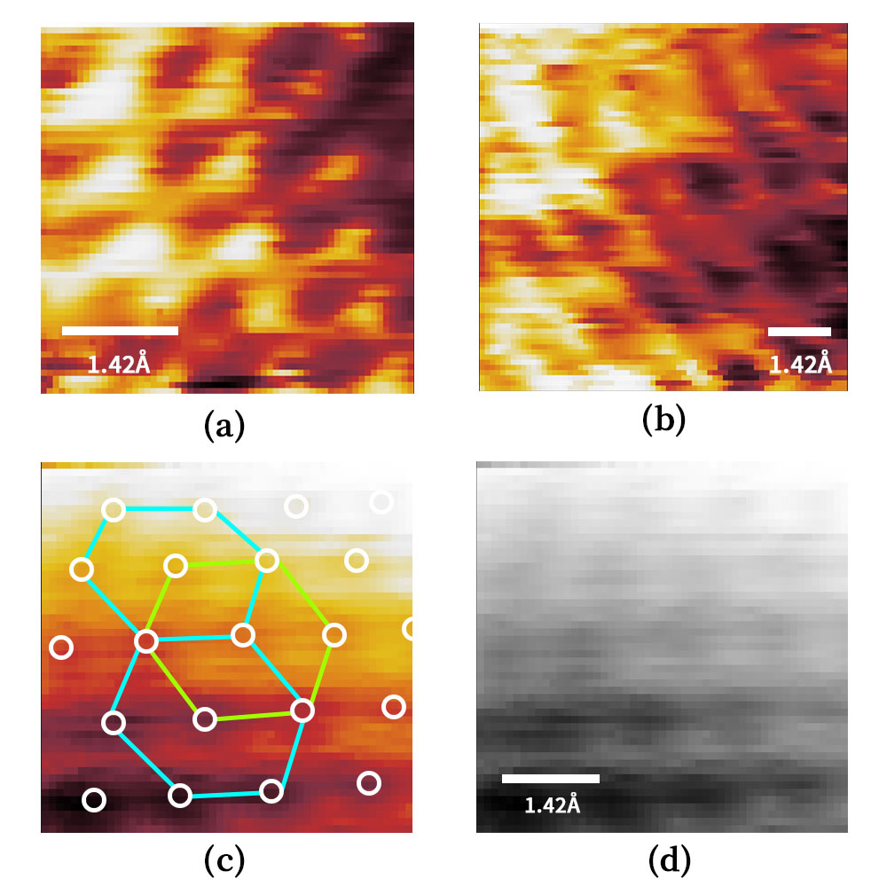
Atomic Imaging of Pyrolytic Graphite (HOPG)
development record
2021/11
unstable tunneling
2022/1/11
Open source page submission
2022/1/18
A is installed under the shock-absorbing table, and the shock-absorbing effect is outstanding
2022/2/05
1) The power supply of the analog part of the system is changed to a 9V battery power supply, and the digital part continues to use a switching power supply.
2) The ADP5070 is not working, Grandma's! Why.
3) In "Construction of a scanning tunneling microscope for imaging of carbon nanotubes" P35, it is found that the tunneling current should be 100pA - 10nA. According to the multiples of the existing op amp, the signal within 1V should be paid attention to. It seems that I made a mistake before.
4) The open-loop voltage gain of OPA627 is 120dB, and the input bias current is 1pA. Reasonably, it should be feasible to use a 100MΩ feedback resistor?
2022/2/16
The input and output characteristics of the op-amp are tested, which proves that the pre-stage tunnel current amplifier circuit is feasible.
2022/3/14
1) The new structure of CNC machining is completed
2) Abandon LVGL and display as a control system
2022/3/21
Tunneling current approach tests were performed using new structural systems, electrical circuits, and control systems:
1) The tunneling current is initially stable and can last for more than ten seconds.
2) Through the sampling test of eight points, the tunneling current-piezoelectric ceramic deformation curve is found to conform to the exponential characteristic.
3) Confirm that a very complicated damping system is not required.
4) It is confirmed that the output jumping phenomenon that appeared before is the mismatch of thermal expansion.
2022/4/12
1) After adjusting the thermal isolation of the stepper motor in the approach mechanical structure, the tunneling current has been very stable and can be maintained for at least 30 minutes.
2) Analyzing the new tunneling curve, it is found that the relationship between the current piezoelectric ceramic deformation is not just a simple exponential relationship. Combined with the opinions given by the teacher, it is suspected that there are other functions compounded. It is initially suspected that it is caused by the capacitor formed between the needle tip and the sample.
3) The fine approach control algorithm has been improved, and now you can click to start the approach and play a few polar fights.
4) The power supply of the analog part is replaced by a 3S lithium polymer battery from a 9V battery.
2022/4/20
The STM image scanning in the constant height mode has been completed and verified by repeated experiments, but the image scale and the complete reliability of the imaging content cannot be determined.
2022/5/01
Write a graduation design thesis.
2022/5/04
70% of the graduation design thesis is completed, and the constant current scanning algorithm is started.
2022/6/16
The open-source information of the second-generation microscope is released
2022/10/21
Start Designing Stick-Slip Piezo Motors
2022/10/26
Improve technical documentation
2023/1/4
The reconstruction of the third-generation circuit and mechanical structure is completed, the design of the stick-slip piezoelectric motor is completed, and it is entering the debugging stage (not released yet, to be released after verification).
(1) Circuit power supply: The reconstructed circuit adopts the scheme of ADP5070 and low-noise LDO to provide multiple power rails (dual ±12V, 5V). ADP5070 uses Zimi 35W dual C-port power adapter for a 5V power supply (the reason is that The power supply ripple is extremely low, the peak-to-peak value is around 13mV, and it appears as a sawtooth).
(2) In terms of PCB layer design: the new generation circuit board is divided into three parts: power board, MCU board, and control board. The power lines are connected between the boards by coaxial signal lines, and the data lines are connected by IDC cables.
(3) Circuit improvement: The MCU board continues to use ESP32 as the controller, but the module model is updated to ESP32-S3, and there is a WIFI antenna slot for future upgrades. Most of the design of the control board remains unchanged in the second generation, and the scheme of AD5761+OPA2227 continues to control the scanning head. However, due to the introduction of the piezoelectric slide stage, the control board additionally adds AD8761 as a DAC for biasing the sample. The DAC originally used to apply the bias voltage is now used to control the piezo slide.
(4) In terms of mechanical structure design: the overall size of the new generation of mechanical structure is reduced, and a stick-slip piezoelectric slide table is introduced for a rough approach (refer to the article "Open-source XYZ nanopositioner for high-precision analytical applications"), and the The pre-amplifier is fully shielded with metal to further reduce noise coupling.
2023/1/18
The MCU module was replaced with ESP32-WROOM-32E, and there were some problems in the compilation of the S3 module, which cannot be solved temporarily due to the lack of data.
In addition, to improve the efficiency of the MCU, the development framework is changed from Arduino to ESP-IDF (from the simple GPIO flip code, the speed of Platform IO + Arduino is 800Khz, the speed of Arduino IDE is 1.2Mhz, and the speed of Platform IO + ESP-IDF is 1.44 Mhz).
2023/2/12
The modification and verification of the third-generation circuit and mechanical structure were completed.
At present, the upper computer and control program are being reconstructed. So far, the PID control of the probe approach has been realized. Compared with the previous generation design, the current is more stable, and the problem of temperature drift has been greatly improved.
2023/03/31
1) Some problems encountered in the assembly of the piezoelectric slide table were found: Although the assembly of the piezoelectric slide table is not difficult, the slide table needs to be kept parallel to a certain degree with the magnet applying pressure during installation, otherwise, the piezoelectric slide table Will not work over long distances.
2) It is planned to design two kinds of piezoelectric sliding table structures to adapt to different shapes of piezoelectric ceramics
3) The software completes the D-I curve test and bias test function
2023/05/02
1) The scan of HOPG is completed, and the fuzzy outline of carbon atoms can be observed.
2) Found an interesting phenomenon: in the process of probing HOPG samples, the tunneling current of the probe will fluctuate (caused by environmental vibration), if the probe sharpness at this time reaches the atomic resolution, the fluctuation curve of the tunneling current will be coupled into a sine-like curve, and after the pin is struck, this coupling will disappear (it is determined that it is not mains interference, the fluctuation period is about 1.4ms, and it will disappear after the pin is struck ).
I think this is because after the probe enters the tunneling distance, driven by the vibration of the environment, the X/Y axis of the probe will move with the vibration, forming a "scanning" effect, and the ups and downs on the surface of the carbon atoms will cause a current periodic change.
2023/05/03
Observation of clear outlines of carbon atoms on HOPG
Reference process
[1] John Alexander: STM Project, http://web.archive.org/web/20121107205242/http://www.geocities.com/spm_stm/Project.html
[2] Dan Berard: Home-Built STM, https://dberard.com/home-built-stm/
[3] Jürgen Müller: Homebrew STM, http://www.e-basteln.de/other/stm/overview/
[4] NanoSurf: NaioSTM, https://www.nanosurf.com/en/products/naiostm-stm-for-nanoeducation
main reference
[1]. Binnig G, Rohrer H. Scanning tunneling microscope: U.S. Patent 4,343,993[P]. 1982-8-10.
[2]. Besocke K. An easily operable scanning tunneling microscope[J]. Surface Science, 1987, 181(1-2): 145-153.
[3]. Ellis M D. Construction of a scanning tunneling microscope for imaging of carbon nanotubes[D]. Texas Tech University, 1998.
[4]. Rogers B L, Shapter J G, Skinner W M, et al. A method for production of cheap, reliable pt–ir tips[J]. Review of Scientific Instruments, 2000, 71(4): 1702-1705.
[5]. 王琦. 高稳定扫描隧道显微镜的研制与应用[D]. 中国科学技术大学,2014.
[6]. Petersen J P, Kandel S A. Circuit design considerations for current preamplifiers for scanning tunneling microscopy[J]. 2017.
[7]. Louis S. Theory of scanning tunneling microscopy[J]. arXiv preprint arXiv:1404.0961, 2014.
[8]. Purdue University. TEM Pictures of STM Tips[EB/OL]. 2002[2022-9-20]. https://www.physics.purdue.edu/nanophys/uhvstm/tip.html.
[9]. Bai C. Scanning tunneling microscopy and its application[M]. Springer Science & Business Media, 2000.
[10]. Nasrollahzadeh M, Sajadi M S, Atarod M, et al. An introduction to green nanotechnology[M]. Academic Press, 2019:199-322.
[11]. Baird D, Shew A. Probing the history of scanning tunneling microscopy[J]. Discovering the nanoscale, 2004, 2: 145-156.
[12]. Merzbacher E. Quantum mechanics[M]. Jones & Bartlett Publishers, 1961.
[13]. 曾谨言. 量子力学导论[M]. 第二版. 北京大学出版社, 2001.
[14]. Grafstrom S, Kowalski J, Neumann R. Design and detailed analysis of a scanning tunneling microscope[J]. Measurement Science and Technology, 1990, 1(2): 139.
[15]. Nam A J, Teren A, Lusby T A, et al. Benign making of sharp tips for STM and FIM: Pt, Ir, Au, Pd, and Rh[J]. Journal of Vacuum Science & Technology B: Microelectronics and Nanometer Structures Processing, Measurement, and Phenomena, 1995, 13(4): 1556-1559.
[16]. Hahn J R, Hong Y A, Kang H. Electron tunneling across an interfacial water layer inside an STM junction: tunneling distance, barrier height, and water polarization effect[J]. Applied Physics A, 1998, 66(1): S467-S472.
[17]. Woo D H, Choi E M, Yoon Y H, et al. Current–distance–voltage characteristics of electron tunneling through an electrochemical STM junction[J]. Surface science, 2007, 601(6): 1554-1559.
[18]. Alexander J D, Tortonese M, Nguyen T. Atomic force microscope with integrated optics for attachment to optical microscope: U.S. Patent 5,952,657[P]. 1999-9-14.
[19]. 陈大任,李国荣,殷庆瑞.逆压电效应的压电常数和压电陶瓷微位移驱动器[J].无机材料学报,1997(06):861-866.
[20]. Fialka J, Benes P, Michlovska L, et al. Measurement of thermal depolarization effects in piezoelectric coefficients of soft PZT ceramics via the frequency and direct methods[J]. Journal of the European Ceramic Society, 2016, 36(11): 2727-2738.
[21]. Instrumentation reference book[M]. Butterworth-Heinemann, 2009.
[22]. Lanza di Scalea F. Measurement of thermal expansion coefficients of composites using strain gages[J]. Experimental Mechanics, 1998, 38(4): 233-241.
[23]. Wijnen B, Sanders P, Pearce J M. Improved model and experimental validation of deformation in fused filament fabrication of polylactic a cid[J]. Progress in Additive Manufacturing, 2018, 3(4): 193-203.
[24]. Oliva A I, Aguilar M, Sosa V. Low-and high-frequency vibration isolation for scanning probe microscopy[J]. Measurement Science and Technology, 1998, 9(3): 383.
[25]. Okano M, Kajimura K, Wakiyama S, et al. Vibration isolation for scanning tunneling microscopy[J]. Journal of Vacuum Science & Technology A: Vacuum, Surfaces, and Films, 1987, 5(6): 3313-3320.
[26]. Walzer K, Sternberg M, Hietschold M. Formation and characterization of coronene monolayers on HOPG (0001) and MoS2 (0001): a combined STM/STS and tight-binding study[J]. Surface science, 1998, 415(3): 376-384.
[27]. Kusunoki K, Sakata I, Miyamura K. Interaction between Tip and HOPG Surface Studied by STS[C]//Analytical Sciences/Supplements Proceedings of IUPAC International Congress on Analytical Sciences 2001 (ICAS 2001). The Japan Society for Analytical Chemistry, 2002: i1267-i1268.
[28]. Chen C J. Theory of scanning tunneling spectroscopy[J]. Journal of Vacuum Science & Technology A: Vacuum, Surfaces, and Films, 1988, 6(2): 319-322.
[29]. El Abedin S Z, Borissenko N, Endres F. Electrodeposition of nanoscale silicon in a room temperature ionic liquid[J]. Electrochemistry communications, 2004, 6(5): 510-514.
[30]. Walzer K, Hietschold M. STM, and STS investigation of ultrathin tin phthalocyanine layers adsorbed on HOPG (0001) and Au (111)[J]. Surface science, 2001, 471(1-3): 1-10.
[31]. Liao H S, Werner C, Slipets R, et al. Low-cost, open-source XYZ nanopositioner for high-precision analytical applications[J]. HardwareX, 2022: e00317.
[31]. Liao H S, Werner C, Slipets R, et al. Low-cost, open-source XYZ nanopositioner for high-precision analytical applications[J]. HardwareX, 2022: e00317.
[32]. De Voogd J M, Van Spronsen M A, Kalff F E, et al. Fast and reliable pre-approach for scanning probe microscopes based on tip-sample capacitance[J]. Ultramicroscopy, 2017, 181: 61-69.
[33]. Wallash A J, Levit L. Electrical breakdown and ESD phenomena for devices with nanometer-to-micron gaps[C]//Reliability, Testing, and Characterization of MEMS/MOEMS Ii. SPIE, 2003, 4980: 87-96.
[34]. Gao C, Kuhlmann-Wilsdorf D, Makel D D. The dynamic analysis of stick-slip motion[J]. Wear, 1994, 173(1-2): 1-12.
Design Drawing
BOM
 Clone
CloneAdd to Album
0
0
Share
Report
Project Members
Intellectual Property Statement & Reproduction Instructions
This is an open-source hardware project. All intellectual property rights belong to the creator. The project is shared on the platform for learning, communication, and research only; any commercial use is prohibited. If your intellectual property rights are infringed on EasyEDA, please notify us by submitting relevant materials in accordance with the Rules for Complaints and Appeals of IPR Infringement.
Users must independently verify the circuit design and suitability when replicating this project. All risks and consequences are borne by the user, and the platform assumes no liability.
Followers0|Likes0
Related projects
 Empty
Empty
Comment