As an amateur music enthusiast who often goes to outdoor places such as parks to practice the piano, I have certain requirements for speakers:
1. With microphone input, supports electret microphones and dynamic microphones.
2. With reverb effect and adjustable effect intensity.
3. Supports playing backing tracks from USB flash drives and playing music via Bluetooth connection.
4. Wear headphones for monitoring, so you don't have to worry about not hearing the backing track clearly and missing the beat in noisy outdoor environments.
5. Can insert a USB flash drive to record the mixed audio during performance at any time.
6. For personal use, the operation is simple. Personal use only requires such as microphone volume, reverb adjustment, backing track volume, and total output volume, while audio recording and playback operations only require buttons such as previous track, next track, play and stop, mode switch, record and stop, etc.
7. The outdoor environment is noisy, so the power must be large enough.
8. Compact in size, lightweight and easy to carry.
In response to the above objectives and requirements, I designed this speaker. Below is a brief introduction, and all materials will be open-sourced for everyone, for the reference of interested friends.
1. Circuit Design
Based on my own practical experience, in terms of functionality, only four potentiometers for microphone volume, backing track volume, reverb amplitude, and total volume are sufficient. After all, we're not using it in professional fields, and professional fields wouldn't take a fancy to civilian speakers that cost a few hundred or a thousand yuan.
The audio player only requires 4 buttons, such as previous track, next track, play and stop, and Bluetooth and USB mode switching, and does not need a display screen, because the tracks used for personal performance are carefully selected by oneself, copied to the USB flash drive in order, and one can tell just by listening with eyes closed. The key configuration of the recording circuit is the same as that of the playback circuit, except that a recording button is defined.
According to the design goal, this circuit is required to provide 4 potentiometers, 2 USB sockets, and multiple tact switches for functions such as playback and recording. If all these components are placed on a single circuit board, the size will be relatively large.
Considering that PCB boards smaller than 10cm in size can enjoy free prototyping service from JLCPCB, I decided to split the circuit into two boards.
-
main board
The main board circuit is responsible for microphone amplification, reverb, pre-mixing, active crossover, power amplification, and power supply, etc., and consists of the following parts:
1.1. Microphone Amplification
The microphone amplifier circuit uses an XC6215 with a high ripple rejection ratio to output 3.3V voltage, providing bias voltage to the electret microphone and powering the low-voltage, low-noise dual operational amplifier HGV722, in order to obtain a good signal to noise ratio.
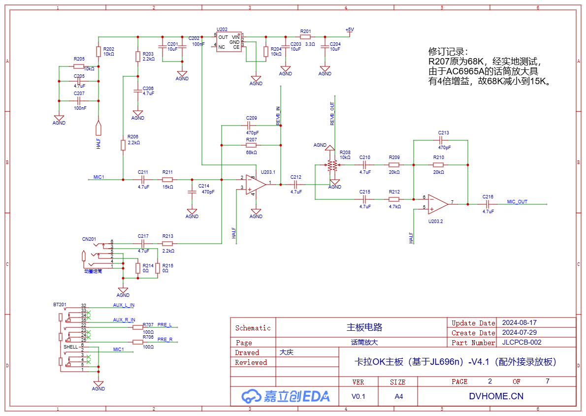
The operational amplifier U203.1 of HGV722 performs inverting mixed amplification on the electret microphone and dynamic microphone. The output is divided into two paths: one path goes directly to potentiometer R208, and the other goes to the reverb circuit REVB_IN, then returns to enter operational amplifier U203.2 for mixed output to MIC_OUT.
After testing, under the same sound pressure, the output of the electret microphone is approximately 7 times that of the dynamic microphone. Therefore, the resistance of the inverting input of the dynamic microphone (R213/2.2K) is approximately 1/7 that of the electret microphone (R211, 15K). Additionally, through actual debugging, the microphone input of AC6965A has approximately 4 times the gain, while the gain of the original designed operational amplifier U203.1 was too large. Therefore, during actual production, the 68K resistor of R207 was changed to 15K.
The connection method of the dual potentiometer R208 here allows the output signal to come entirely from the output of the direct operational amplifier U203.1 when turned fully counterclockwise, and when the potentiometer is turned fully clockwise, the output signal comes entirely from the output of the reverb circuit REVB_OUT. The intermediate state of the potentiometer is the mixed superposition of the original audio and the reverberated audio.
Since the reverb circuit has a 4x voltage gain, the two inverting input resistors R209/20K and R212/4.7K of op-amp 2 differ by approximately 4 times, so that the output volume difference is not significant during reverb adjustment.
1.2. Reverberation
The reverb circuit uses the AC696N series chips from Jieli, implementing only one function - Reverb. This function actually only uses the MIC input and 1-channel DAC output of the chip. The USB socket, pins, buttons, RF antenna socket, etc. in the circuit are mainly reserved for testing, learning, and development purposes, and do not play a role in this circuit, so they can be left unassembled.
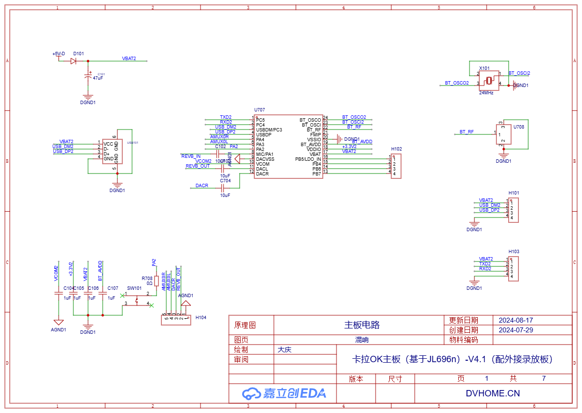
The diode can isolate the power supply when connecting the programmer. Here, it is necessary to design the analog ground AGND and the digital ground DGND1 separately; otherwise, the interference noise of the digital circuit will be very large.
1.3. Mixing Preamp, Headphone Amplifier
HT82V735 is selected for pre-amplification of audio mixing, which combines signals from the line AUX input, the DAC_L2/R2 output of the Bluetooth player, and the microphone preamplifier output, etc., and outputs the mixed PRE_L/R to the next stage.
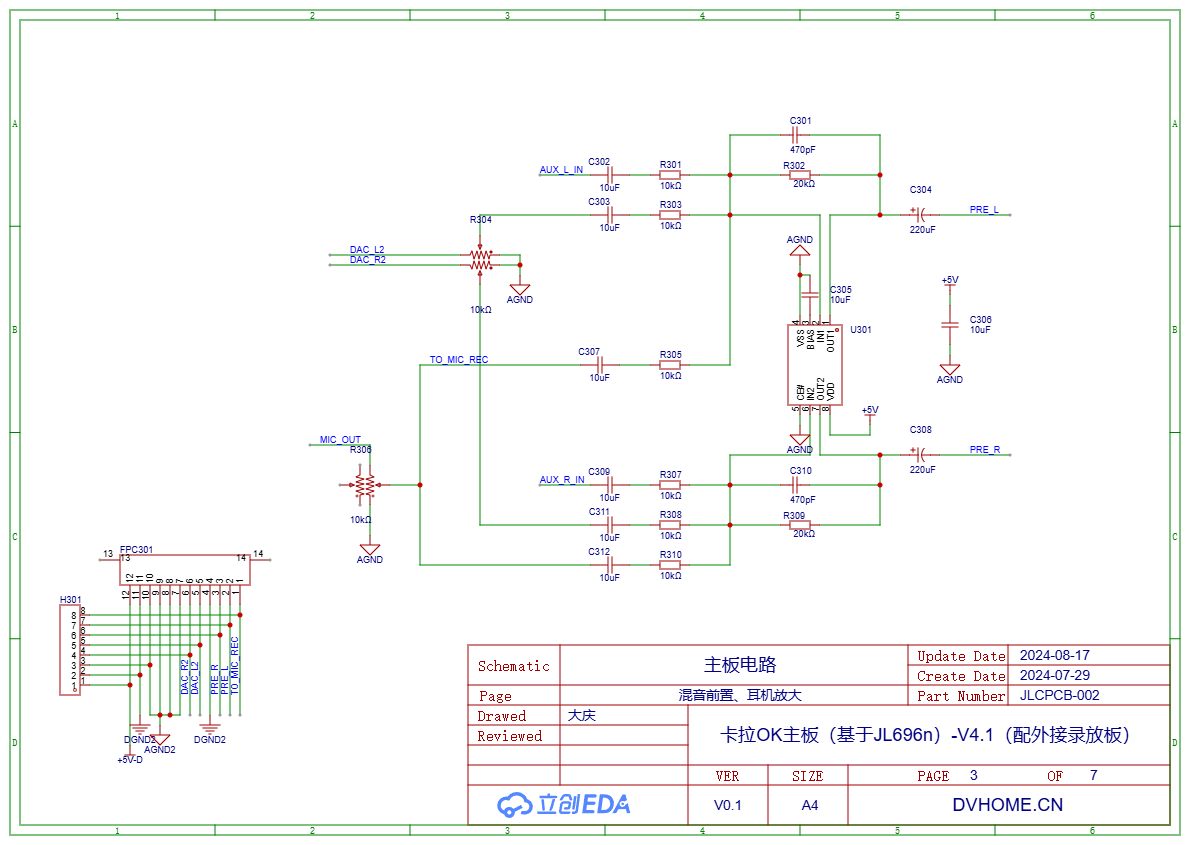
This IC was originally designed for headphone amplifier circuits and can operate at a voltage of 5V. Its pins are not exactly the same as those of a general-purpose dual operational amplifier, but they are similar. If an operational amplifier is used as a replacement, the circuit modifications will be minimal.
The value of the output capacitor should be larger; otherwise, when the headphones are plugged in, the output low-frequency will be significantly weakened due to the relatively low impedance of the headphones.
Here, 12 FPC connectors and 8-pin headers (without soldering the pins) are placed. The impedance of the ground wire is related to the interference noise of Bluetooth. Concerned that the connection impedance of the FPC is not low enough, 4 wires are connected in parallel to the analog ground here. If noise elimination is still not thorough enough, the holes of the headers can also be used for soldering.
1.4. Active Bi-Amplification
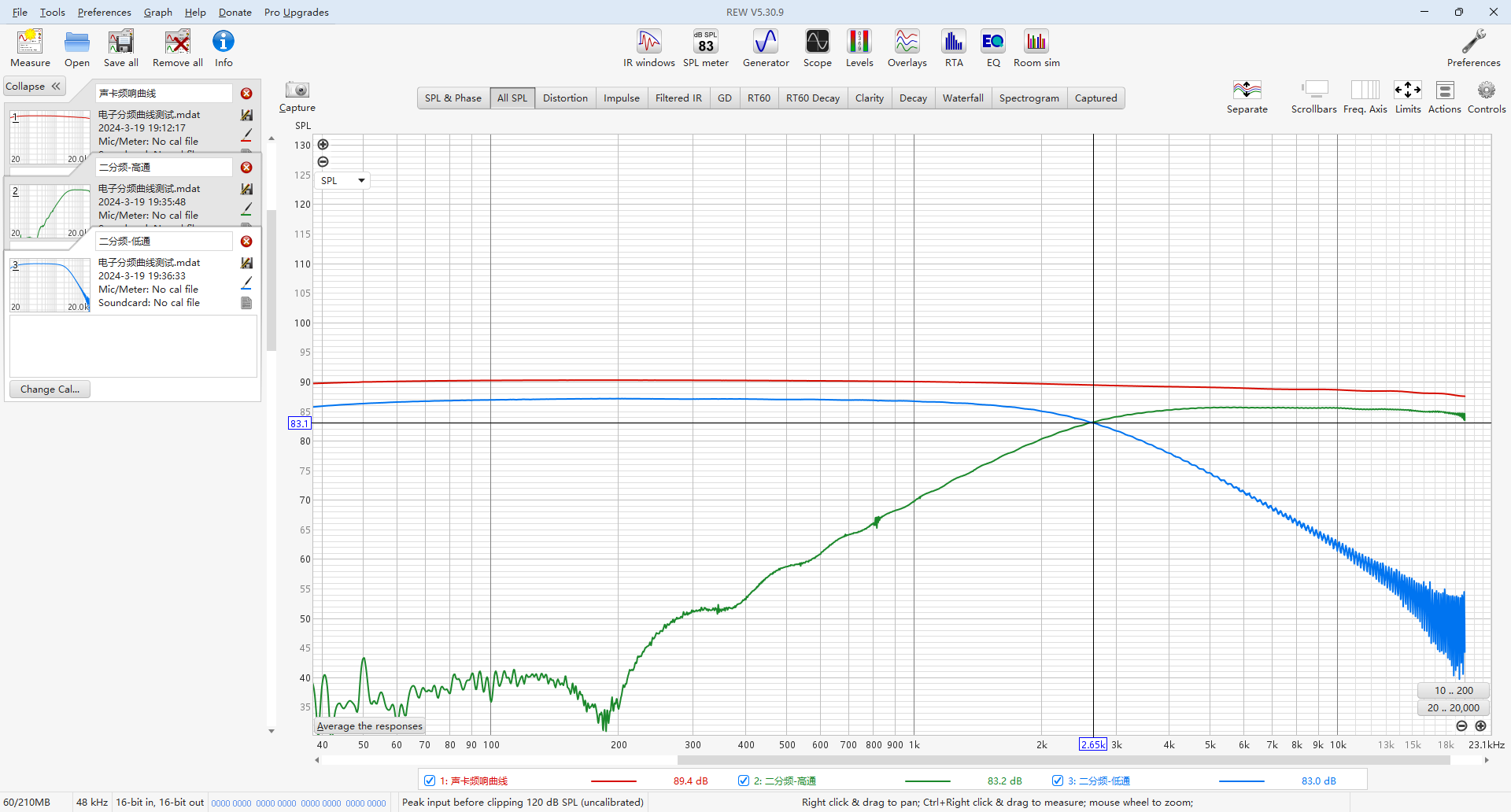
A dual operational amplifier is used to implement high-pass and low-pass 2-way frequency division, with 10nF and 4.3K components, and the crossover frequency is around 2.6KHz. The operational amplifier also uses HGV722.
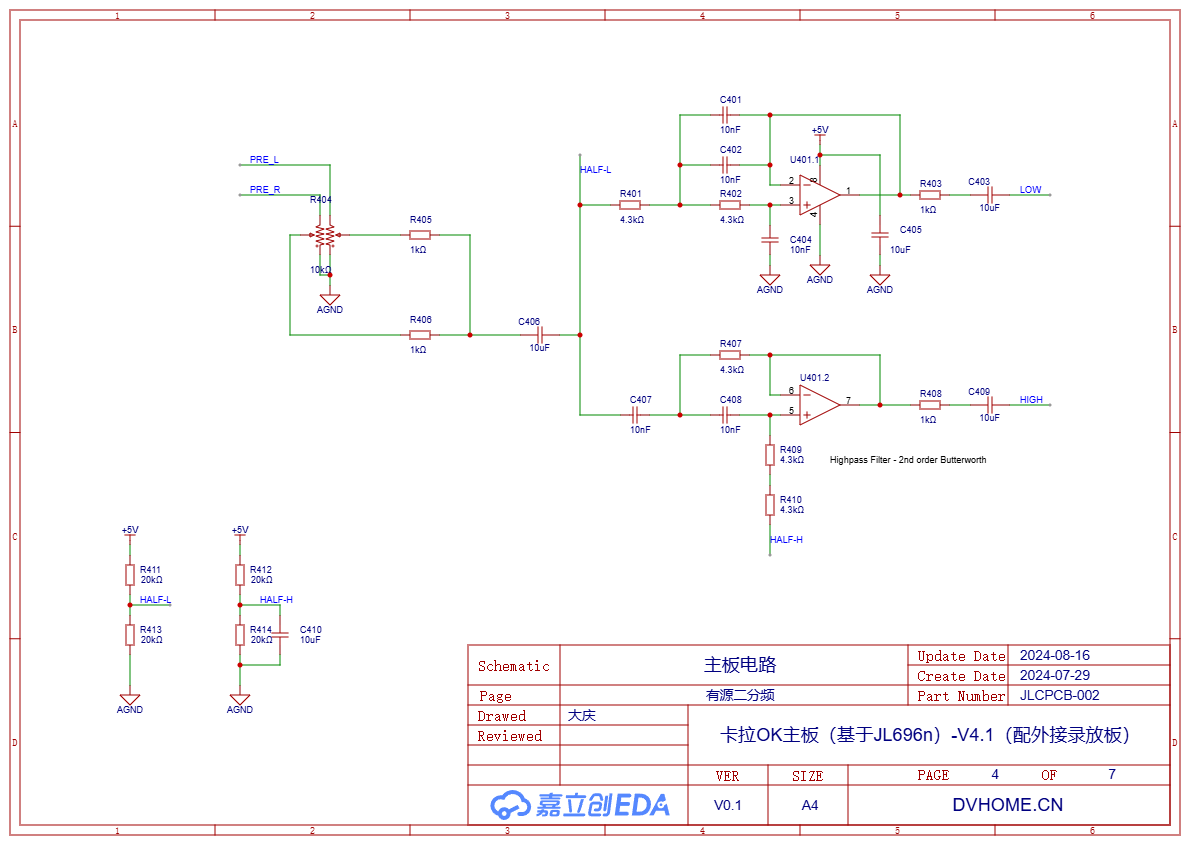
Previously, a frequency division circuit was made using this design drawing and tested with REW, and the results were in line with the design:
1.5. Class D Amplifier
Use TPA3118 to make a two-channel power amplifier, with one channel for the woofer and the other for the tweeter.
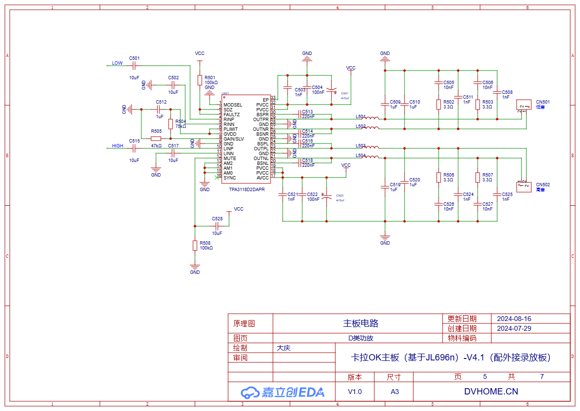
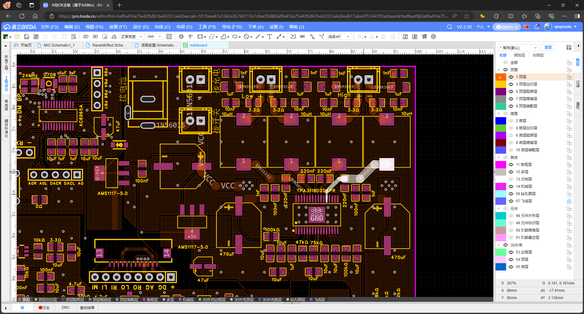
The bottom of TPA3118 should be soldered to a large-area copper foil to facilitate heat dissipation. The extension wires of the power output pins should be as thick as possible to allow large currents to pass through.
1.6. Lithium Battery Charge Indication
How to make a simple lithium battery power display? Here, a dual operational amplifier or comparator is used to detect the voltage. A circuit is built using the standard version of JLCEDA for simulation.
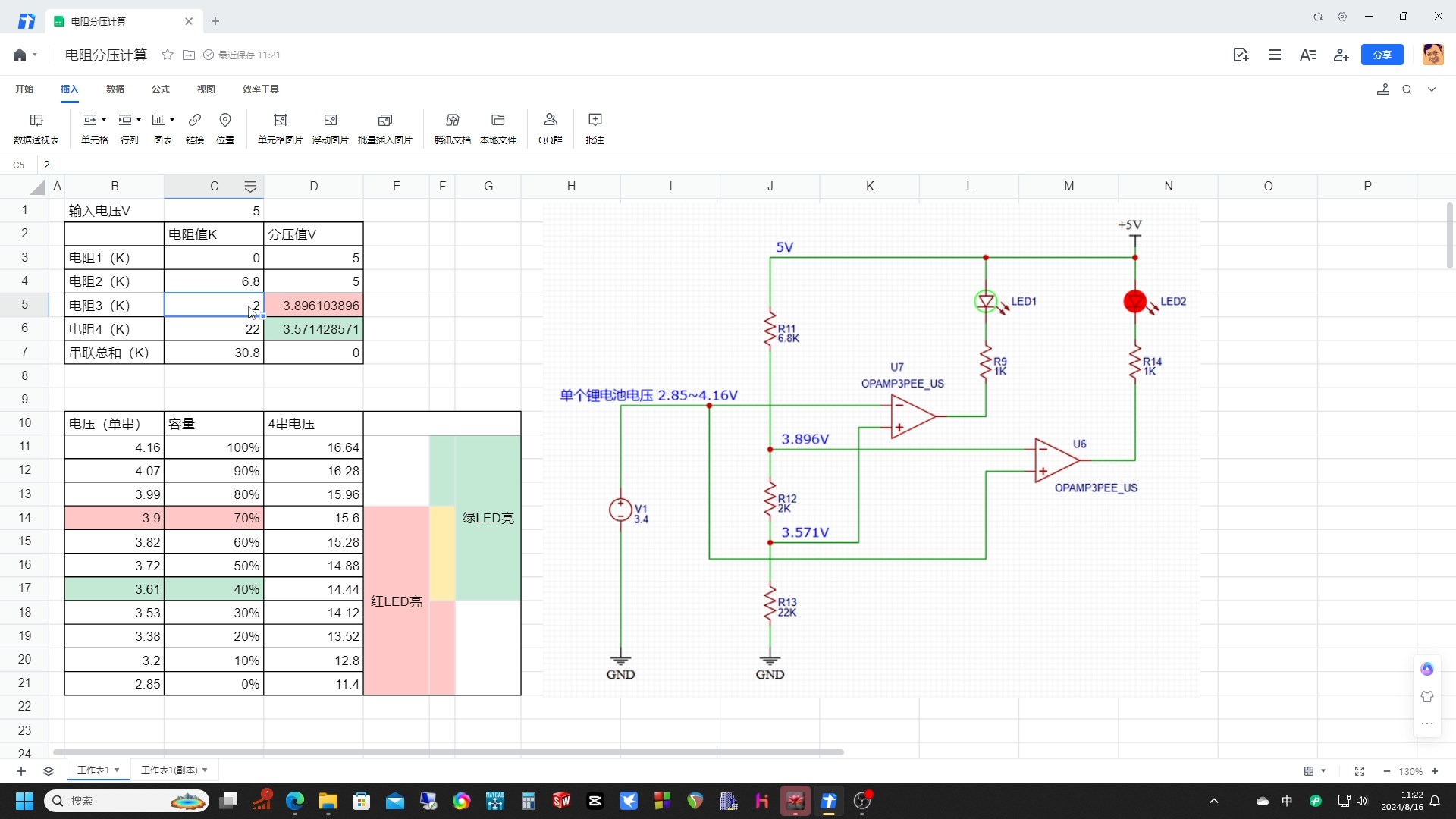
After repeated calculations, resistors with common resistance values of 6.8K, 2K, and 22K were used for voltage division, resulting in 3.896 and 3.571 volts, corresponding to 70% and 30% of the lithium battery's charge. When the charge is higher than 70%, the green LED lights up; when it is lower than 30%, the red LED lights up. Between 30% and 70%, both lights are on, mixing to form yellow.
During actual design, the dual comparator LM293DT is used. For a 4-cell lithium battery, the ratio of R604 to R608 is 3:1, here we choose 39K and 13K, so that the divided voltage is exactly the voltage of a single lithium battery cell. If other numbers of lithium batteries are used, then the ratio of these two resistors can be adjusted.
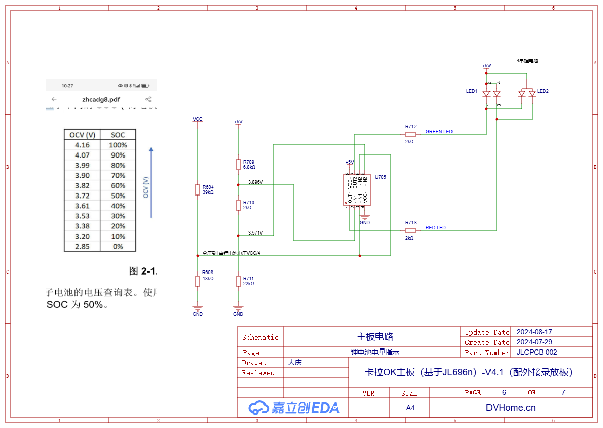
The bi-color LED in the figure is packaged in two forms: side-mounted and through-hole, which are reserved for PCB design, and only one type will be installed during actual soldering.
1.7. Power Supply
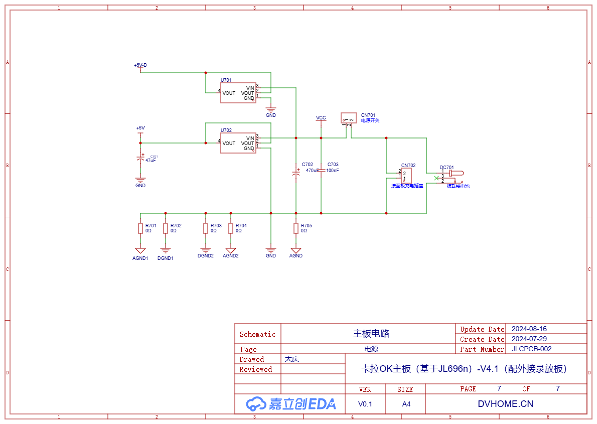
The power supply section uses two 5V voltage regulator blocks to supply power to the analog circuit and the Bluetooth chip. Additionally, there are multiple 0-ohm resistors, which are mainly used for circuit diagramming to distinguish the analog ground and digital ground of multiple circuits. In practice, they do not need to be soldered and can be directly shorted.
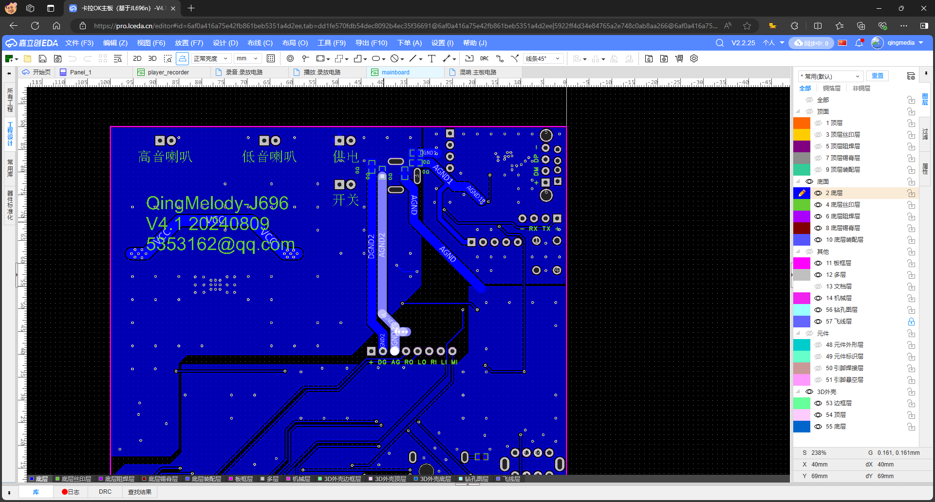
During PCB layout, all analog and digital grounds are routed to the vicinity of the power input. If a 0-ohm resistor is not drawn, it is inconvenient to draw traces. Finally, I covered the 0-ohm resistor with a filled area, which ignores DRC errors when outputting the PCB.
2. recording and playback board
As previously mentioned, separating the recording and playback board was done with consideration of multiple factors such as size, functionality, and so on.
2.1. Recording board
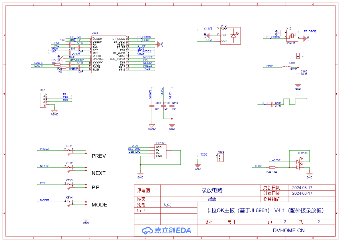
Using the AC6955F chip specifically for recording enables stereo recording in any scenario. Here, only the USB interface is used instead of the TF card slot because a USB flash drive is small, easy to carry, can be hung on a keychain, and is convenient to use, unlike a TF card which is so small that it's not easy to find and requires a card reader to use.
Since there are enough IO ports, the buttons of the SDK are set to the IO mode, which can save a few resistors. Although resistors are inexpensive, the fewer components for manual soldering, the better.
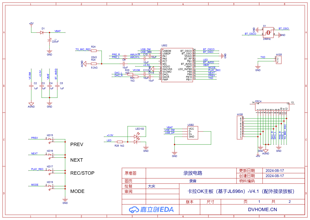
For easy disassembly and assembly, we tried using FPC connectors. Since we had never used them before and didn't know how the line impedance would be, we specifically used multiple parallel cables here as the AGND analog ground connection to reduce the impedance of the analog ground as much as possible. This is because the interference in the Bluetooth section is quite significant, and if not handled properly, the noise will be very large.
2.2. Playback board
Use the same model AC6955F for playback, with the key and LED pin configurations the same as those for recording, so that the relevant settings of the SDK program will be the same.
2. Panel Design
Export the 3D models of the PCB main board and the recording and playback board,
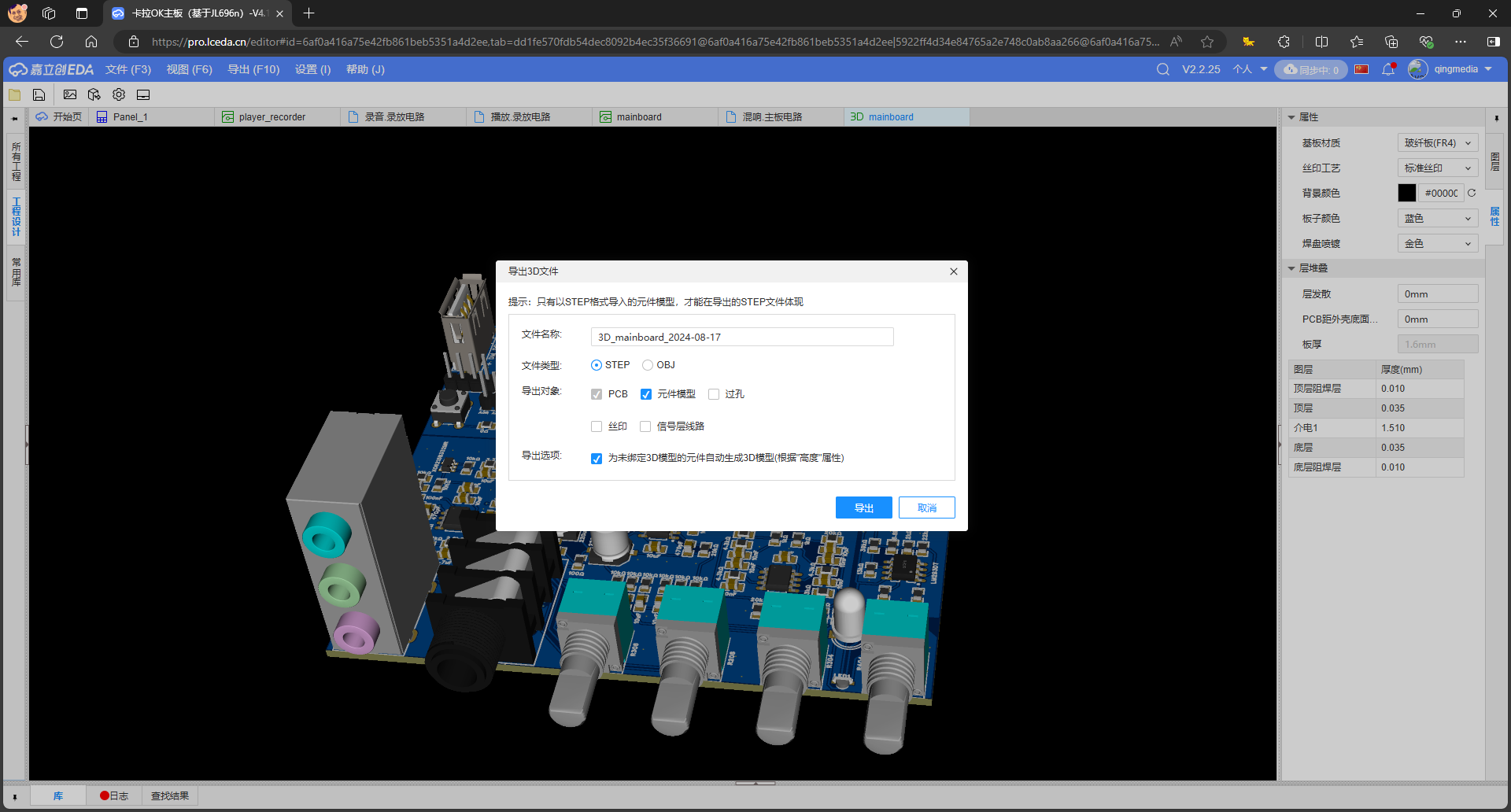
Open it with SolidWorks. What needs attention during this process is that SolidWorks is prone to crashing, mainly because there are many parts in the 3D model of the PCB, and some parts have an error or compatibility issue. That's why I once suggested to JLCPCB that when exporting the 3D model, one could choose which parts to export. In fact, when making a panel or other designs, there is no need to export all the parts.
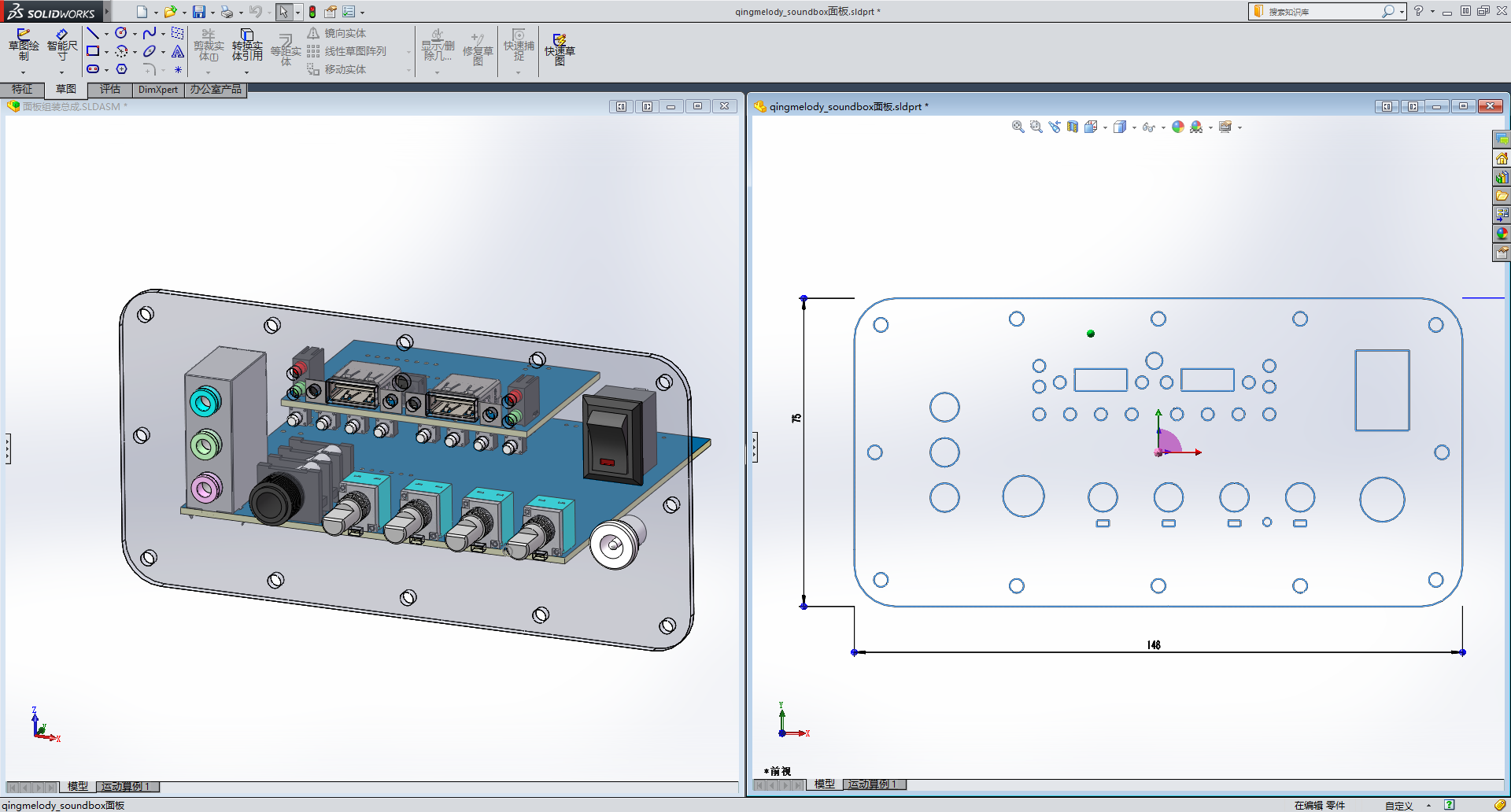
Then, based on the relevant dimensions of the potentiometer, socket, etc., design the opening dimensions of the panel, etc. After completion, export the DXF file.
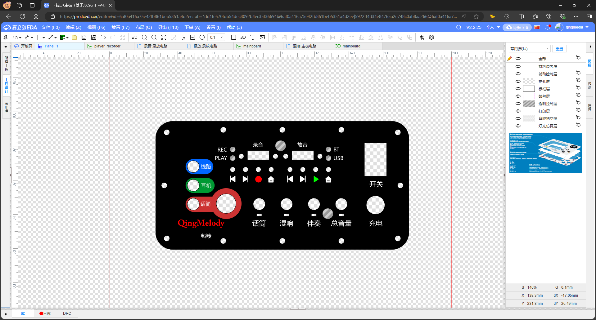
Create a panel in the JLCPCB EDA project, import this DXF file, and then proceed with panel design, mainly including opening holes, transparent windows, text, fill colors, etc.
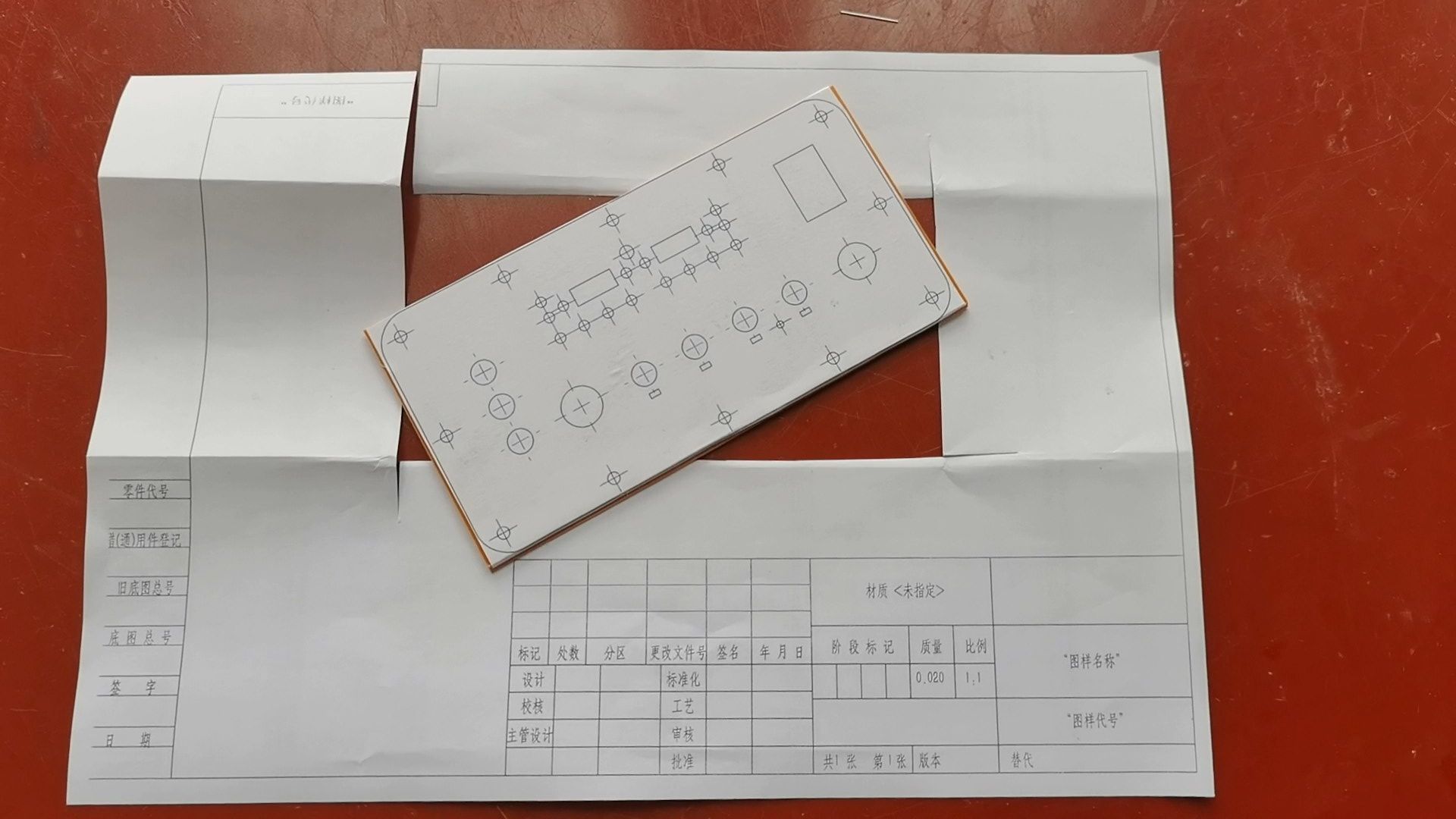
I've decided to manually make a panel out of bakelite. The method is also simple: print the panel design from SolidWorks onto paper, then cut it out and paste it onto the bakelite board.
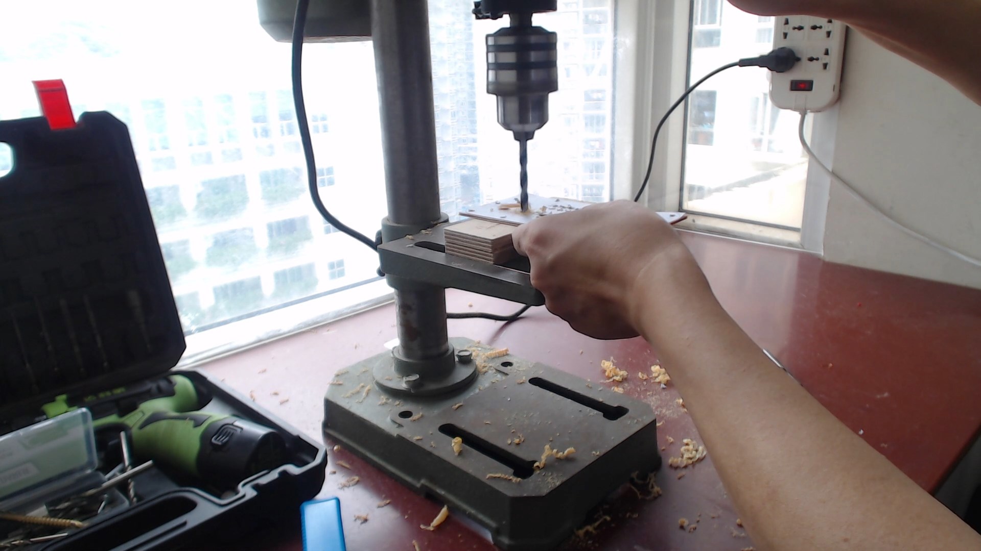
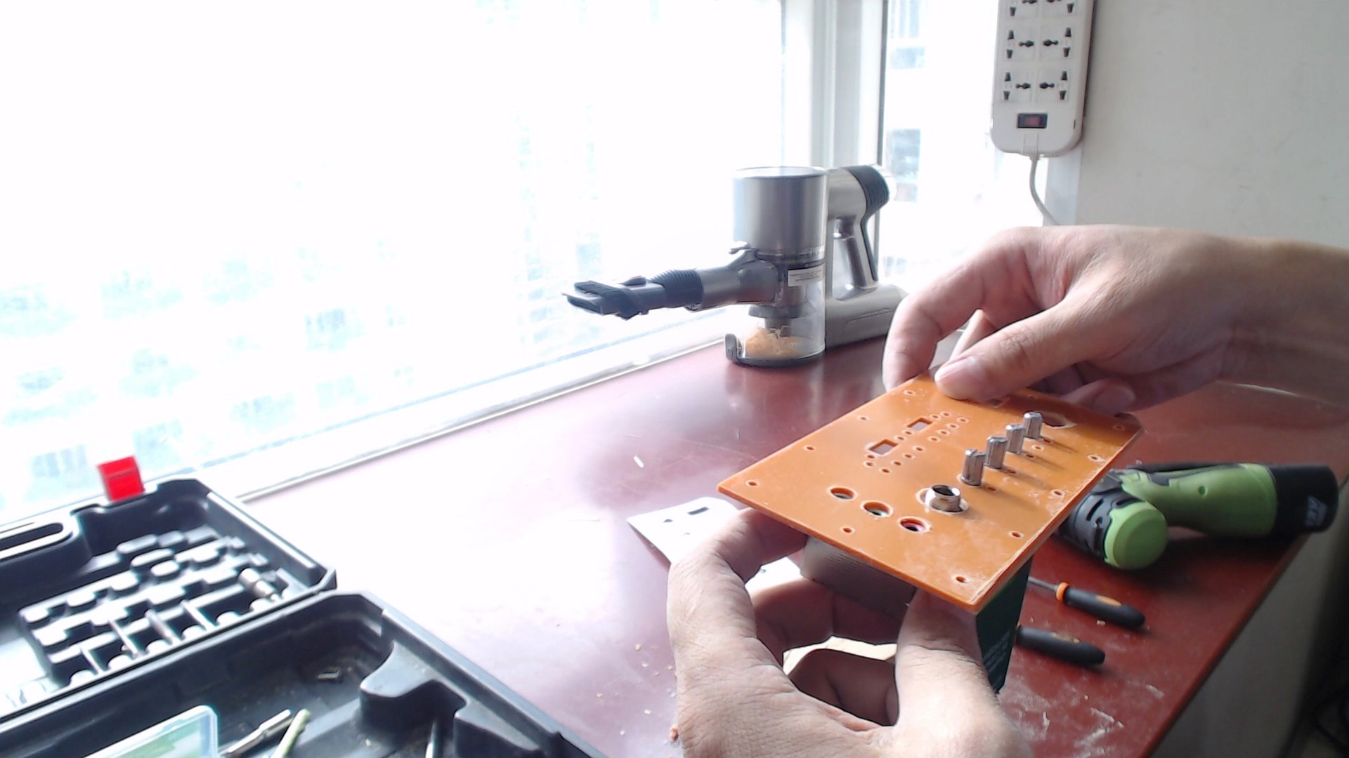
Then drill holes with an electric drill and use a set of files to shape square holes.
3. Box Design
The enclosure is designed using SolidWorks, with the edges of the panels designed to have interlocking concave and convex shapes similar to a mortise and tenon structure, and the speaker is protected by a fan mesh cover.
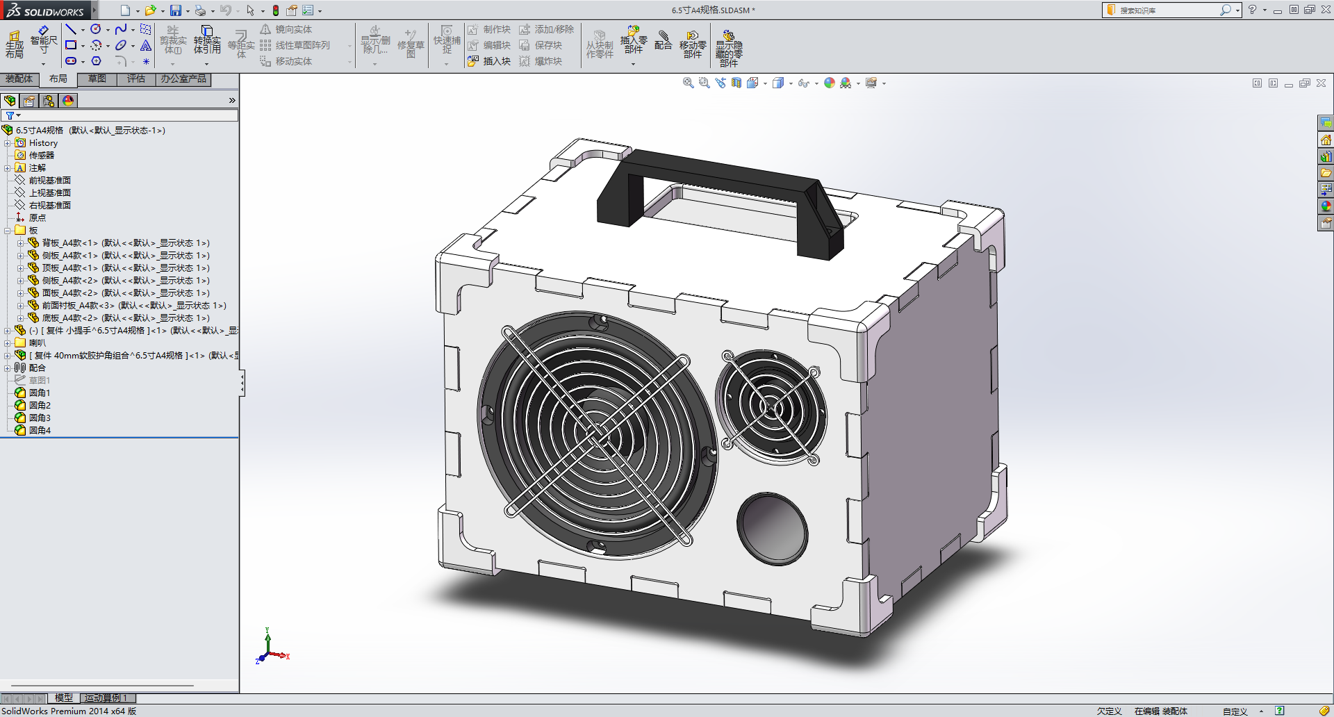
Then create a panel file for all the boards and export the AutoCad format drawing file for processing.
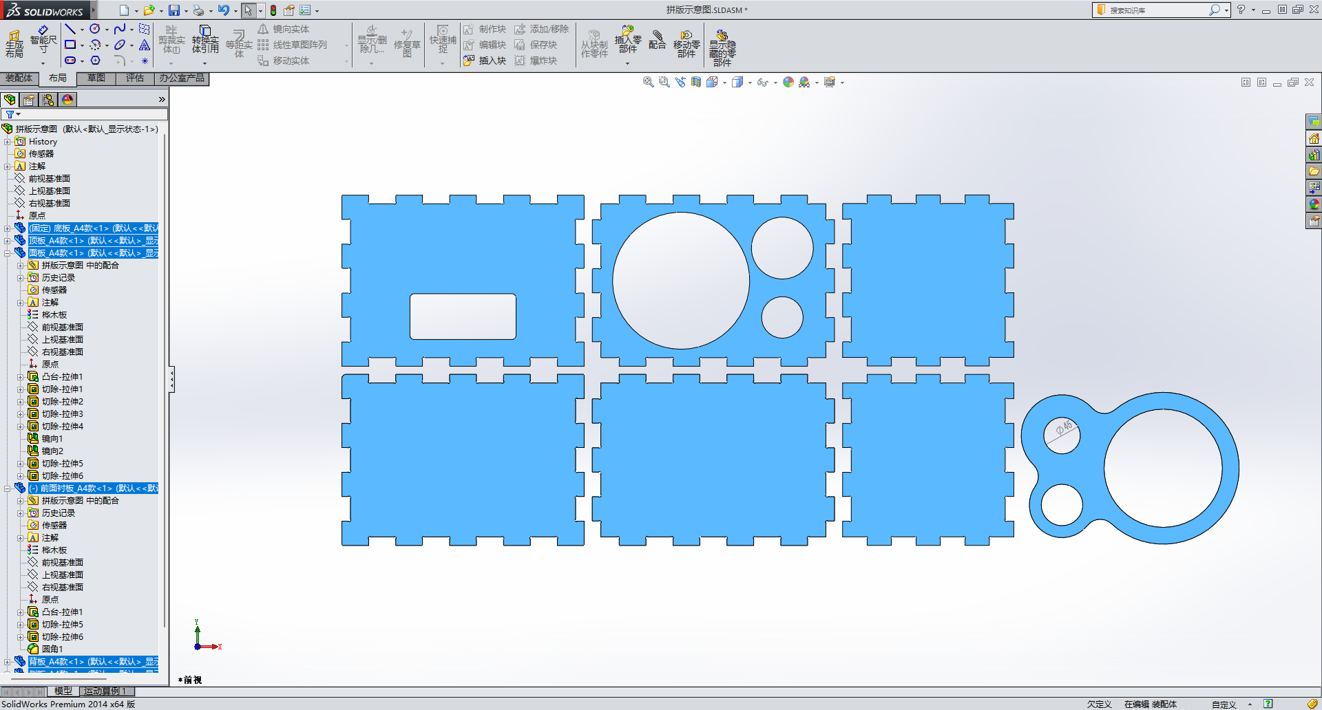
Finally, contact the merchant, send the processing drawings for the merchant's CNC cutting.
4. Assembly and Debugging
1.PCB soldering
Thank JLCPCB. This time, I was lucky enough to receive a free SMT coupon for PCB prototyping:

Then, let's do the SMT (Surface Mount Technology) for the speaker main board with the most components, and only make a prototype of the recording and playback board.
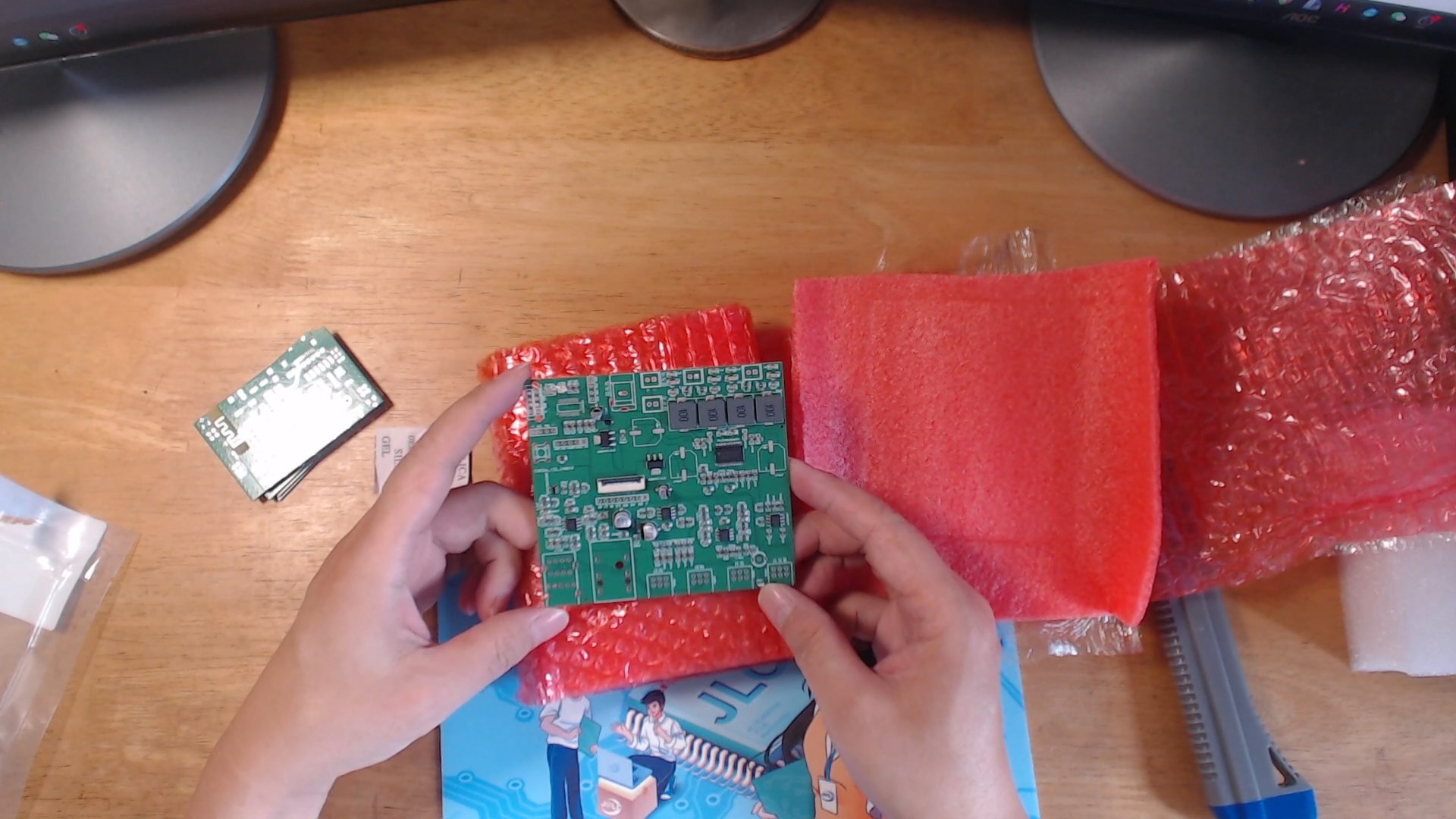
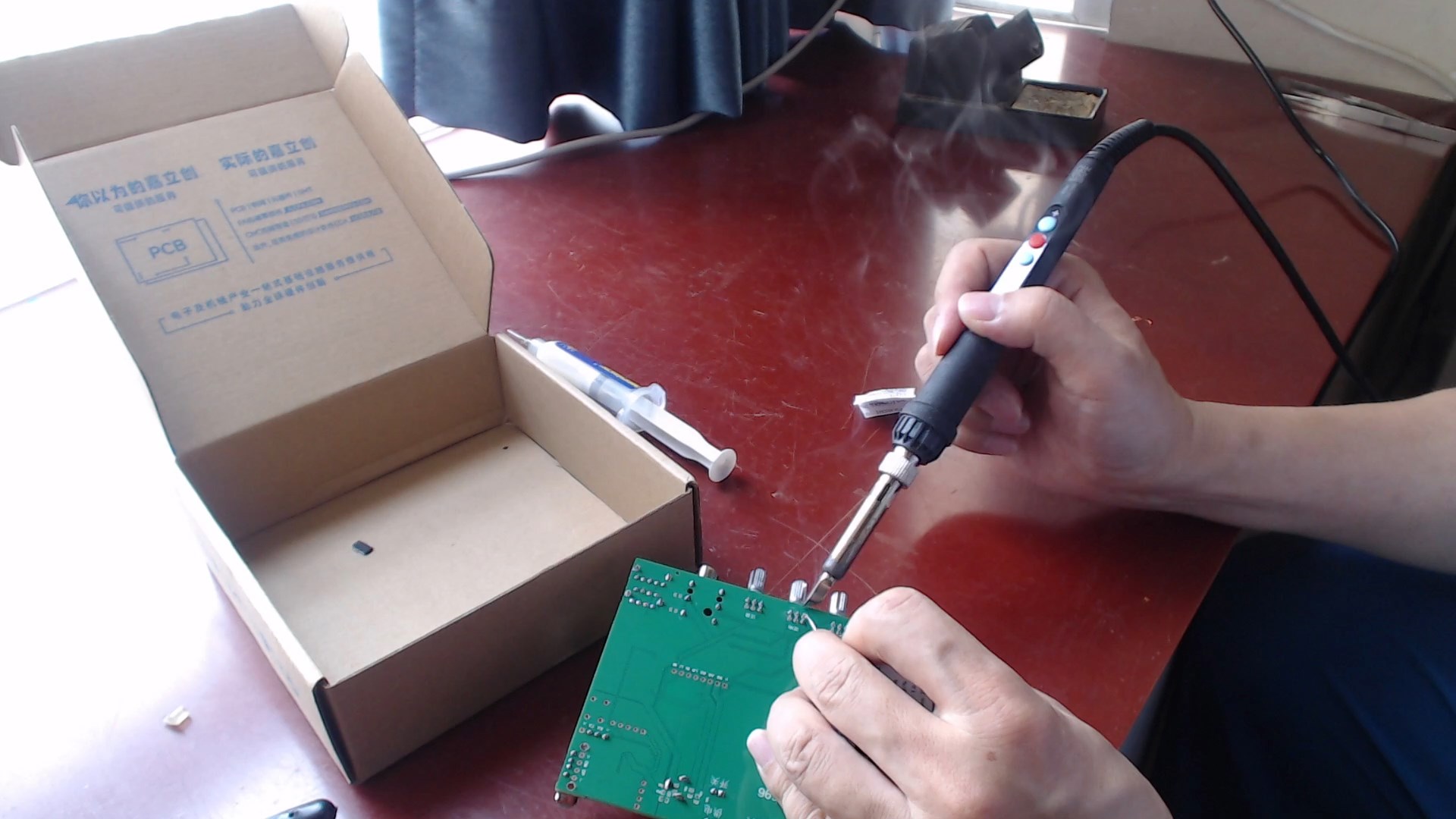
The recording and playback board has a simple circuit with few components, which are soldered by hand with point soldering and surface mounting, and then welded using a heating station. The main board has relatively more components, and luckily I got a free SMT coupon, so it was surface-mounted at JLCPCB, but the component cost was equivalent to several meals. The AC6965A chip is not available in the JLCPCB store, so this chip was hand-soldered later, and other discrete components such as potentiometers also need to be hand-soldered.
2. SDK Modification, Compilation, and Flashing
This circuit uses 3 Jieli Bluetooth chips, each performing 3 functions respectively, so the SDK program is also divided into 3 parts, which are modified, compiled, and flashed separately.
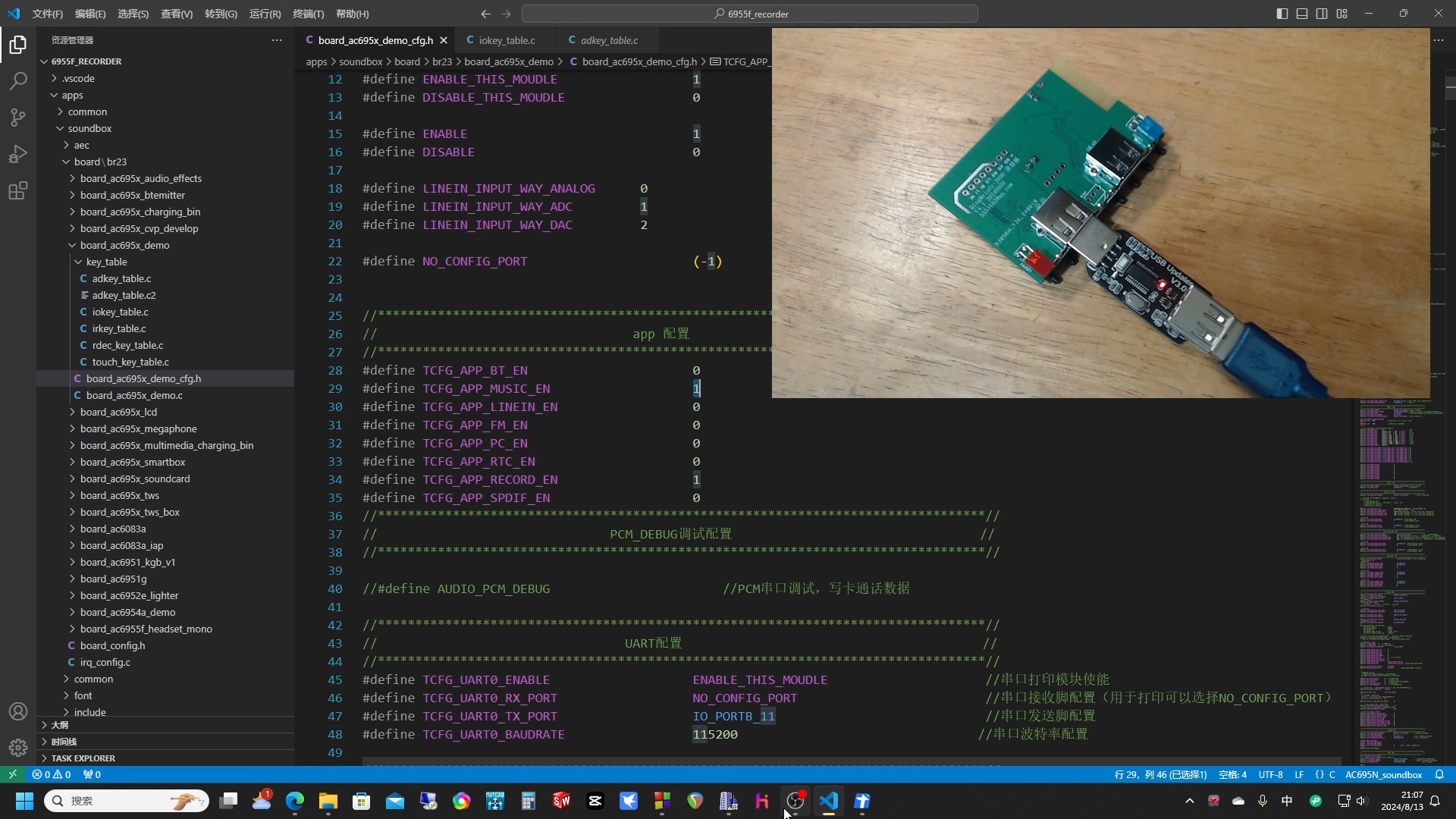
Some may wonder why other people's speakers can use just one chip. This is because the computing power of Jieli's chips is limited. If a single chip were used to perform the above functions, it would always be unable to achieve a balance.
3. debugging
After connecting the two boards with the programmed firmware, attaching the speaker and power supply, and powering on, the tests of the reverb effect, player, and recording all achieved initial success.
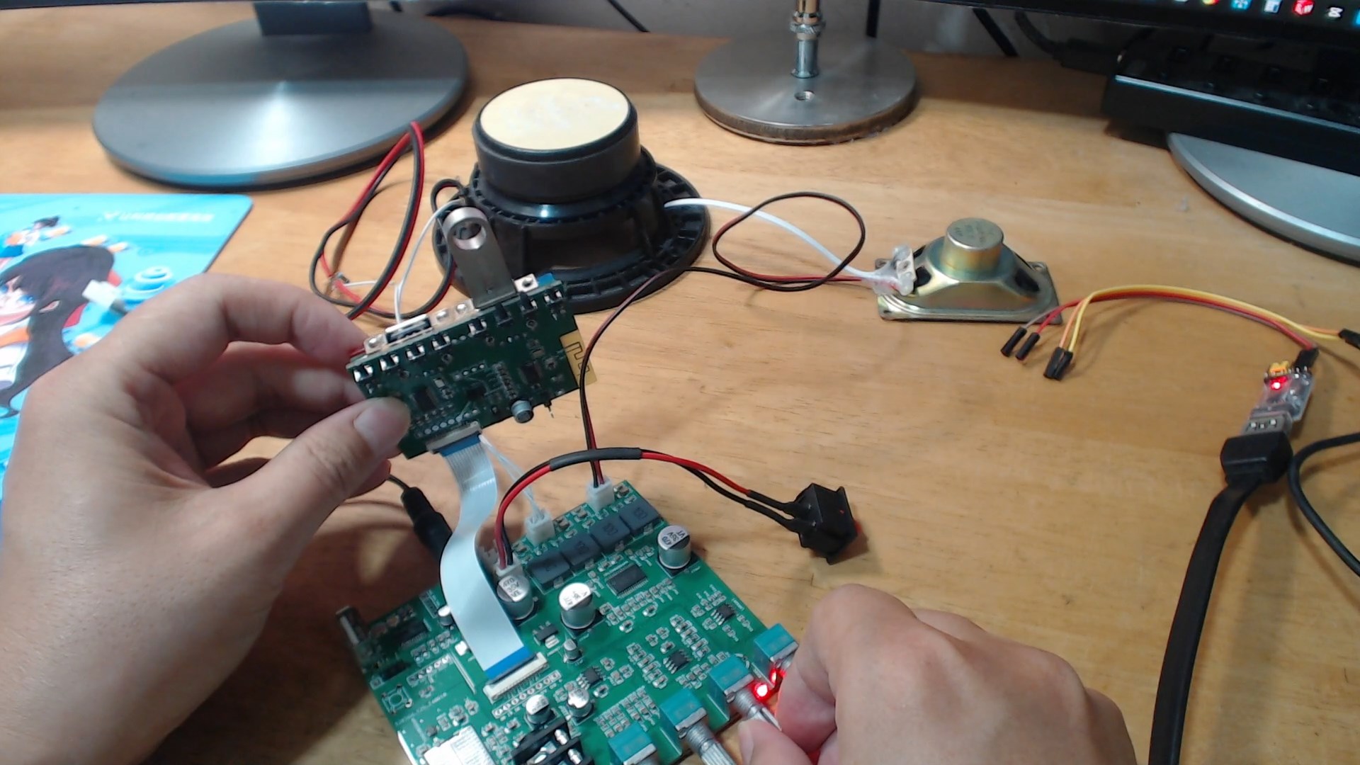
Retesting the player was also successful.
Then the recording function was tested and it also succeeded.
To facilitate the insertion and removal of USB flash drives, the circuit is installed on the panel.
During debugging, the free audio editing software Audacity was used to generate an audio file of a 1KHz sine wave with maximum amplitude,
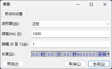
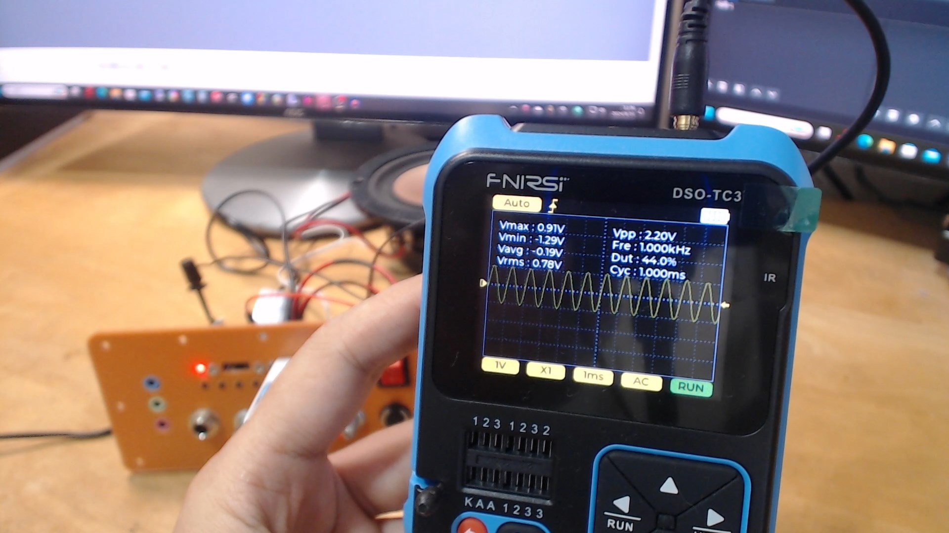
After saving to a USB flash drive, play it using the USB flash drive, measure the output signal of the playback board with an oscilloscope, the waveform is undistorted, and the amplitude Vrms is around 0.78V, which is still relatively ideal.
To verify the lithium battery power display circuit, a variable power supply was specifically purchased and connected to the main board.
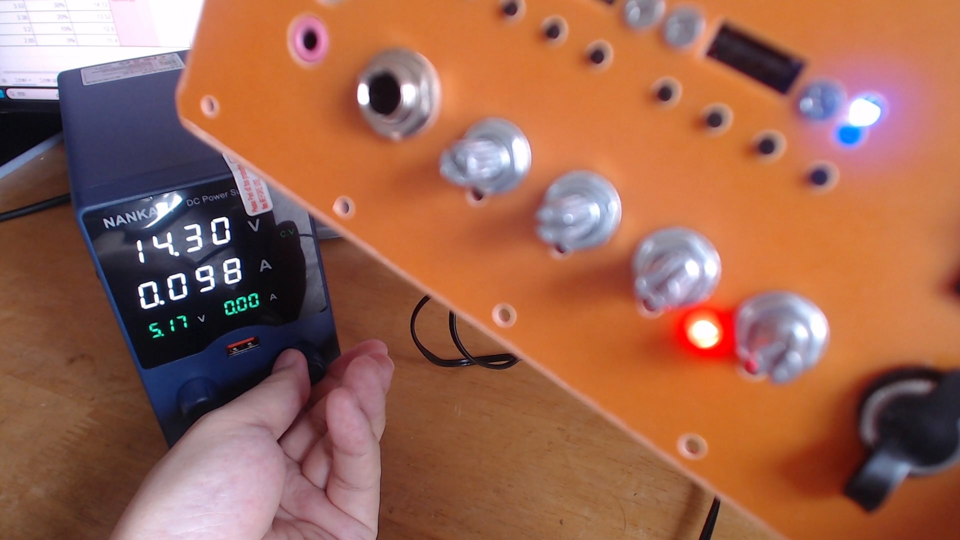
When the output voltage is adjusted from 16.8V to 15.7V, the dual-color LED light changes from the green LED being lit to both the red and green LEDs being lit (here, the dual-color LED is a side-mounted type, and the synthesized yellow is not very obvious). When the voltage continues to drop to 14.3V, it turns red. The results indicate that it is very close to the predetermined 15.6V and 14.44V, meeting expectations.
4. Packing, sound testing, and recording
The assembly of the speaker enclosure is skipped here, which contains 4 strings of lithium battery packs,
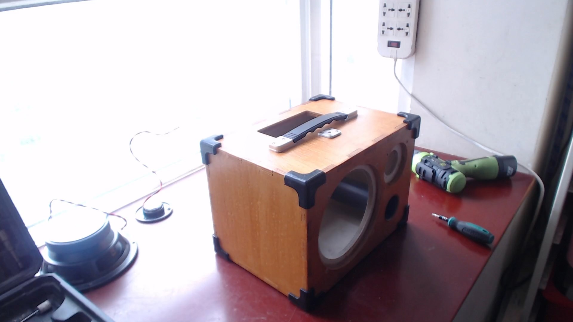
This design involves installing and fixing the operation panel from the inside, which results in the volume being semi-hidden on the surface of the box panel. In this way, when the box is turned over, since the handle has a certain height, the volume will not be hit. Of course, it is also possible to install it from the outside inwards, which is even more convenient.
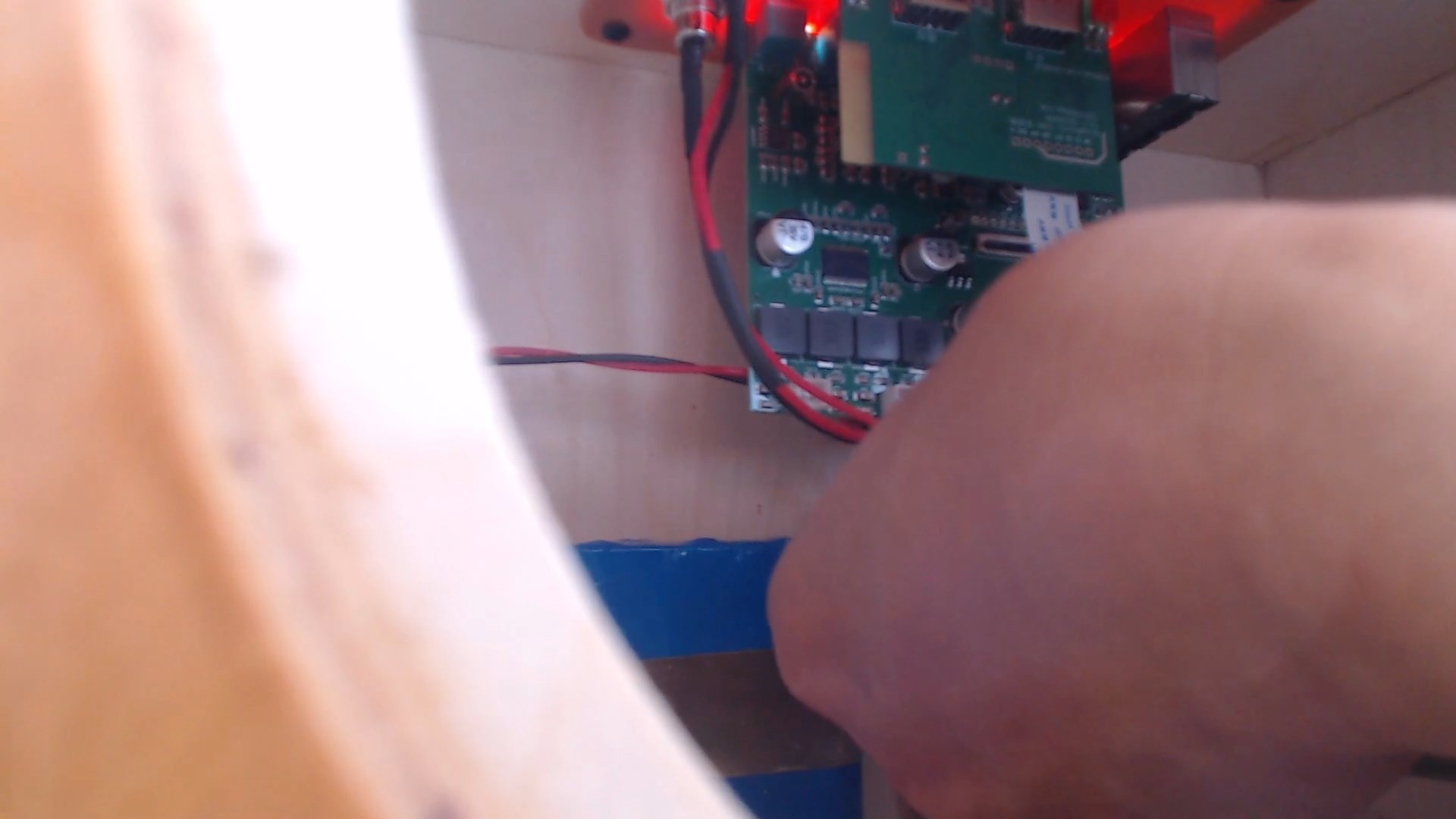
First, install the panel, then mount the circuit board onto the panel, and secure the nuts of the potentiometer and socket.
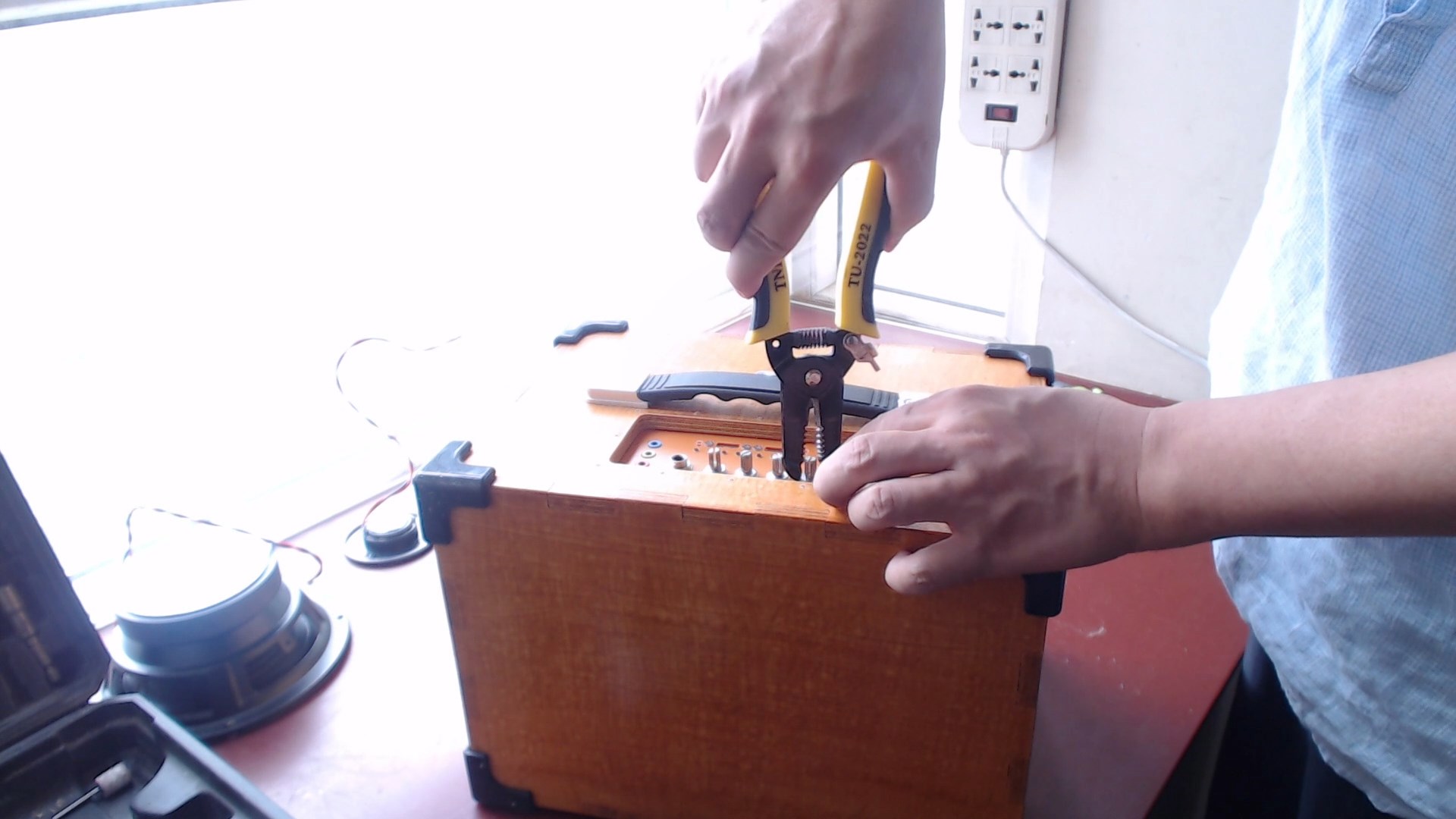
Insert the battery output wire, woofer, and tweeter wire into the main board, place sound-absorbing cotton inside the box. Secure the speaker screws and install the protective mesh cover. Put on the potentiometer cap.
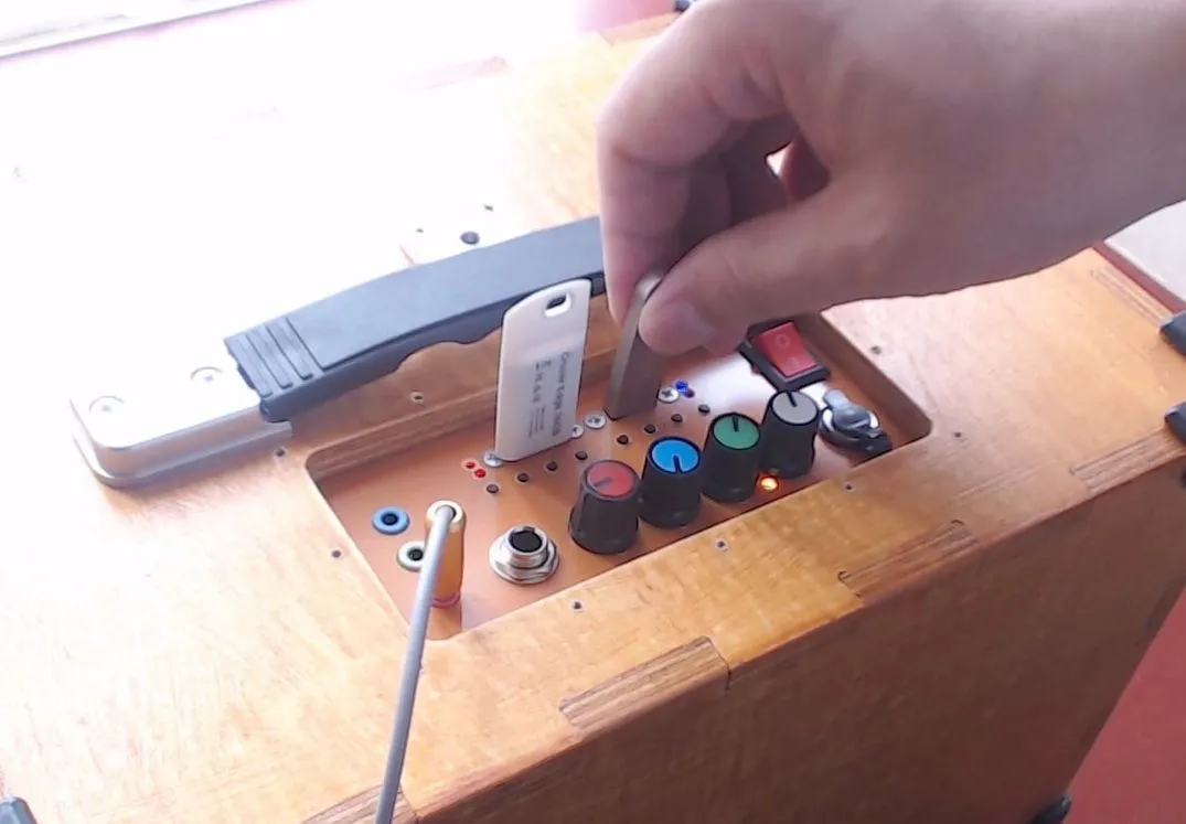
The USB socket on the right is dedicated to playback, while the one on the left is for recording. Insert a blank USB flash drive, click the button to switch to recording mode, and press the record button to start recording.
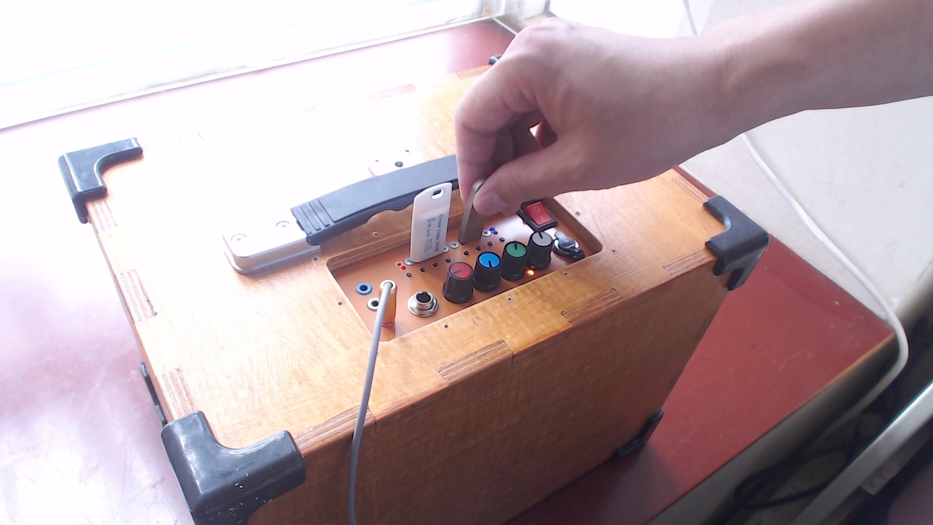
2 microphone sockets, 3.5mm for plugging in electret microphones, with adjustable volume and adjustable reverb level.
After the audition, it fully meets the design expectations! Reverb can be added when using the harmonica.
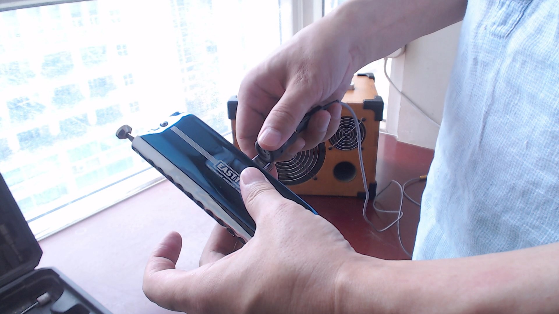
When using an electronic wind instrument, since the instrument comes with built-in reverb, you can set the reverb to off.
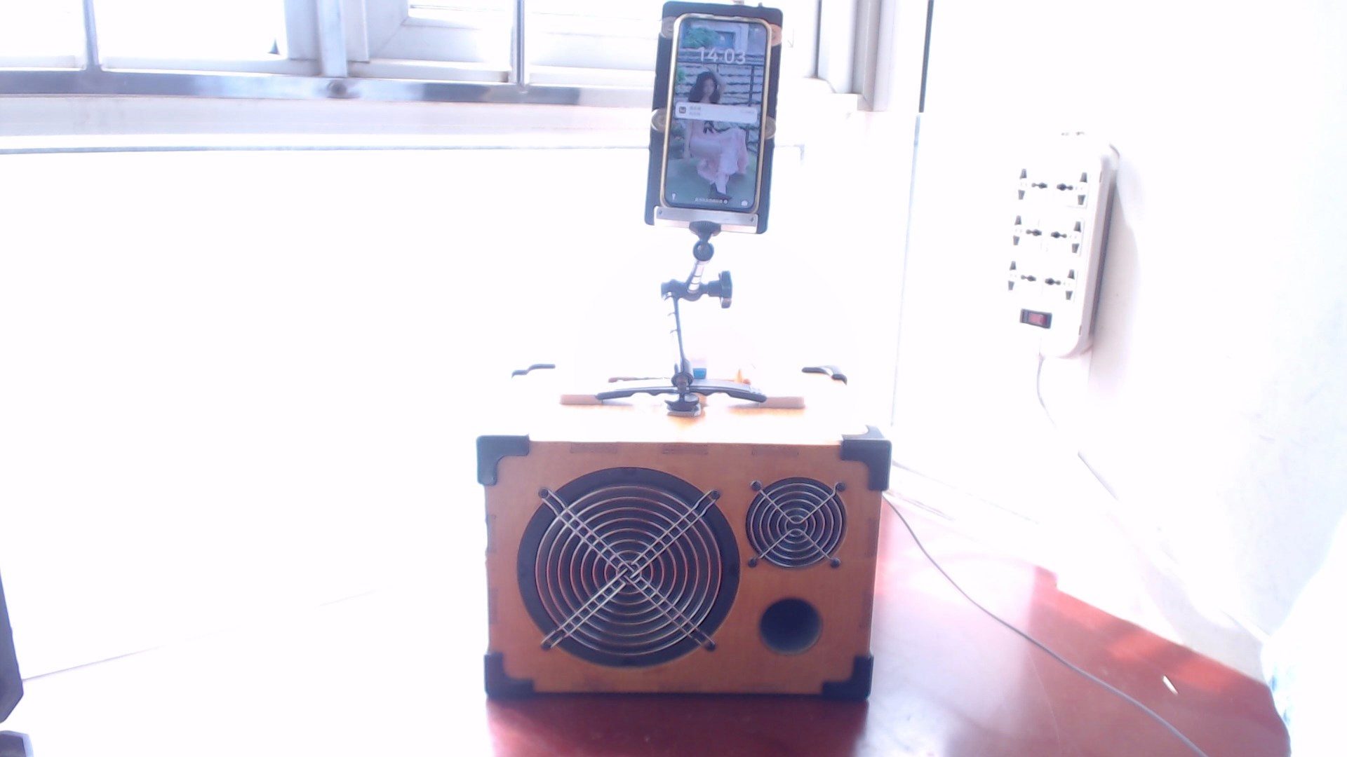
5. Information Sharing
Jieli chip program and enclosure design files are shared on Gitee at gitee.com:
 Completed
 Develop a multi-functional roadshow speaker with recording, reverb, and Bluetooth functions using Jieli chips


 The preview image was not generated, please save it again in the editor.
 Empty
Empty


Comment