

 Ongoing
Evalaution-competence-CAO-DAO
STDEvalaution-competence-CAO-DAO
9
0
0
0
Mode:Full
License
:Public Domain
Creation time:2025-09-25 06:34:37Update time:2025-09-29 01:16:52
Description
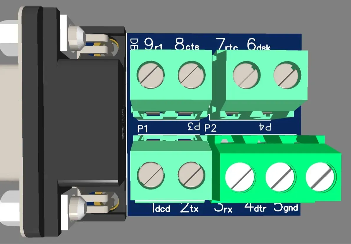
This schematic is a passive breakout board that fans out a DE‑9 (DB9) D‑sub connector to multiple screw terminal blocks. The nine signal pins of the DB9 (DB1) are routed one‑to‑one to four pluggable 5.08 mm terminal blocks:
- P1: 2‑position terminal block
- P2: 3‑position terminal block
- P3: 2‑position terminal block
- P4: 2‑position terminal block
The D‑sub’s metal shell/mounting lug is tied to GND to provide shielding and chassis reference; there is no active circuitry, level shifting, or protection on the signals. The board simply exposes each DB9 pin on convenient terminals to ease wiring, testing, and prototyping of devices that use a DB9 interface (e.g., RS‑232/industrial equipment).
Notes:
- Connector references: DB1 = D‑SUB‑DR‑9PCM‑BB (DE‑9), P1–P4 = WJ500V‑5.08 series terminal blocks.
- Verify the pinout required by your device (e.g., which DB9 pins are TX/RX/GND, etc.) and assign them to the desired terminal positions accordingly.
- The ground symbol indicates the connector shield (and/or designated ground pin, depending on your final wiring) is bonded to PCB ground for noise/EMI control.
Design Drawing
BOM
 Clone
CloneAdd to Album
0
0
Share
Report
Project Members
Followers0|Likes0
Related projects
 Empty
Empty
Comment