

 Completed
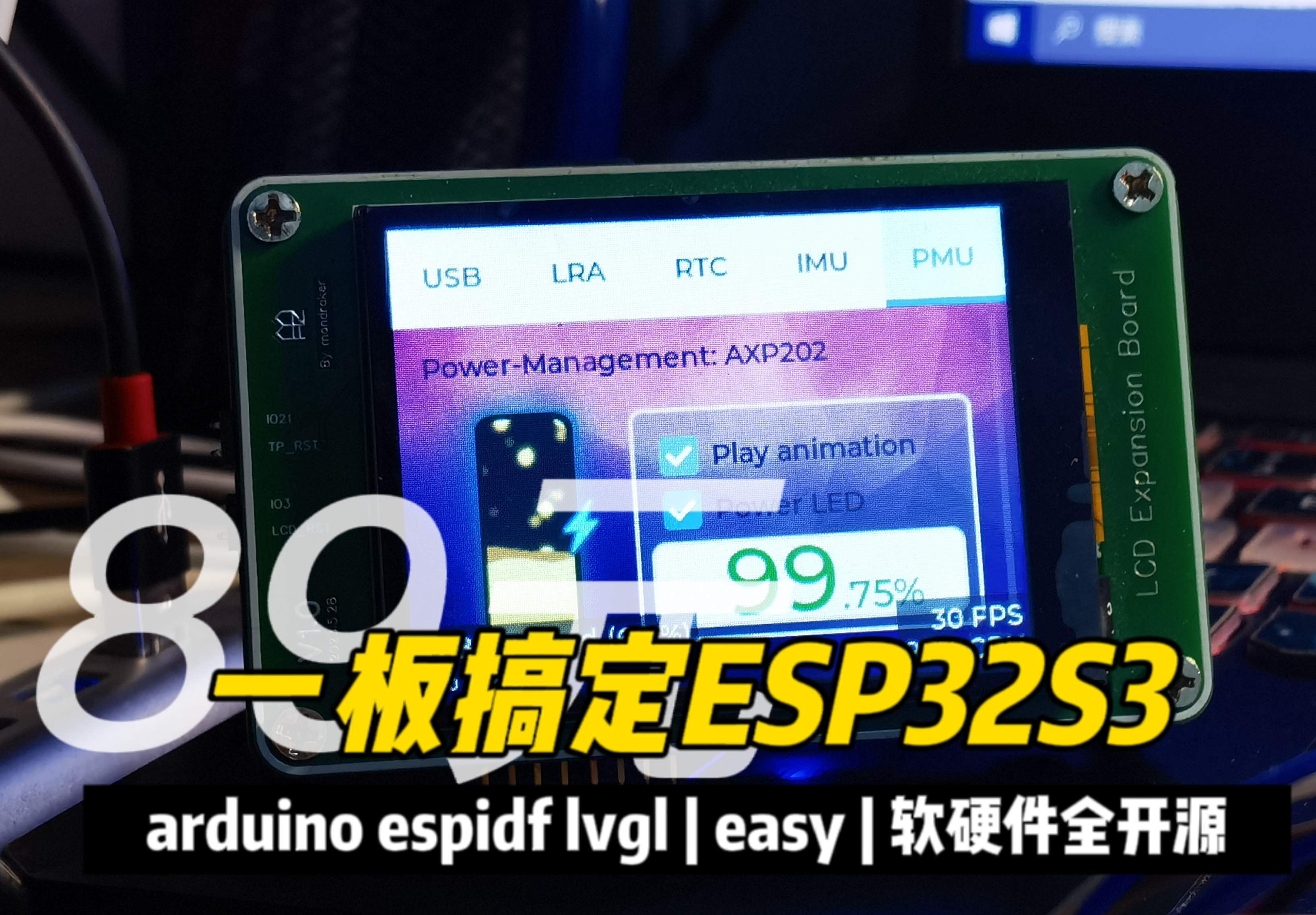
[What you want] ESP32S3 full functional development board
PRO [What you want] ESP32S3 full functional development board
638
0
0
0
Mode:Full
License
:GPL 3.0
Creation time:2024-10-15 05:37:47Update time:2024-10-15 09:27:51
Description
Designed by mondraker (from OSHWHub)
Link:https://oshwhub.com/mondraker/jiu-shi-ni-xiang-yao-de-nei-zhon
Design Drawing
Add to Album
0
0
Share
Report
Followers0|Likes0
Related projects
 Empty
Empty
Comment