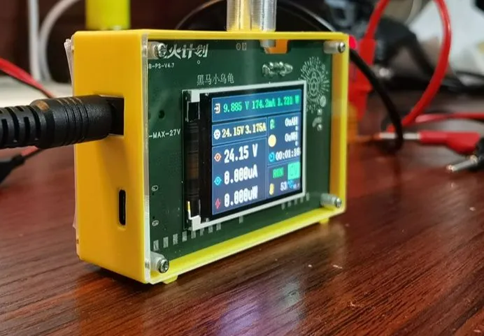
 Completed
USB adjustable power V3, hardware V4.7 comprehensive upgrade
PRO USB adjustable power V3, hardware V4.7 comprehensive upgrade
License
:GPL 3.0
Description
Important updates and precautions
———————————————————————————————————————————————————————————
- The hardware of this project has been fully updated to V4.7 version, which mainly updates the following contents:
1. Added input anti-reverse connection/backfill, output anti-backfill, can directly charge the battery, don't worry about current backfilling.
2. The output current limit of SC8701 is added, and the high-side MOS tube is used to achieve double current limiting, which improves the serious problem of heating up when the high-side MOS tube works at large pressure difference.
At the same time, it avoids the problem that SC8701 cannot limit the current when it is short-circuited.
3. Added an external NTC circuit, and later added this part of the software function.
- Precautions
1. This version of the hardware needs to open the project, and then you can see the hardware version of V4.7. As follows:

2. The software version required for this version must be greater than or equal to V2.7.
3. It is recommended that the Type-C port and DC port do not supply power at the same time.
The current input anti-backfill circuit is not mature,When the voltage is high, there is a risk that the adapter may reverse the series, and the adapter will be damaged!!
The reason is that the Vebo withstand voltage limit of the triode, the voltage difference between the two input ports needs to be less than about 5V, and the third transistor may break down after exceeding, resulting in the reverse series of the two input sources.
Interested in hands-on ability can try to make the following modifications, should be able to improve this problem, because there is not enough verification, everyone is free to play.

Project Brief Introduction
———————————————————————————————————————————————————————————
This design supports USB PD3.0, BC1.2 protocol, and can make the USB power adapter that supports PD/BC1.2 protocol output 5V, 9V, 12V, 15V, 20V through PD/BC1.2 protocol.
The power supply supplies power to the system;
Wide range of output voltage, adjustable from 2.0V ~ 34V, more than 5A load capacity, 10mA~8A current limit continuously adjustable;
The input voltage and current, the output voltage and current are monitored in real time, and fed back to the user through the 320X240 TFT screen or the host computer;
Simple interaction mode, only through a rotary encoder or host computer to adjust the output voltage and current limit;

(Click on the image to enlarge it)
WeChat applet on the upper computer.
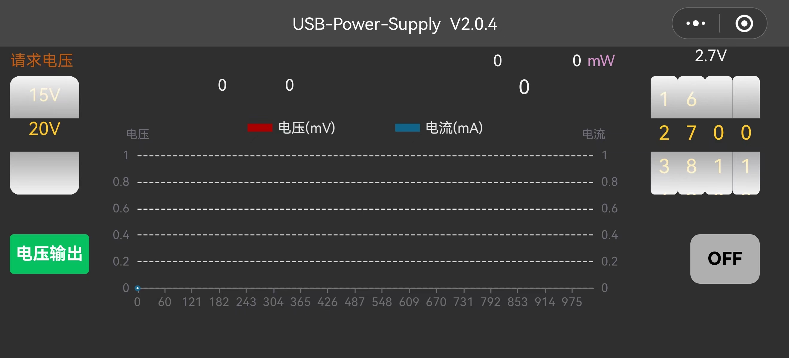
(Click on the image to enlarge it)
The Mini Program is online, and you can scan and open the Mini Program:

Project Background
———————————————————————————————————————————————————————————
- In the last two years, I have only come into contact with open source hardware projects, because I don't have much experience in open source projects, and my hardware development ability is limited, so in V1 and V2 versions
stepped on a lot of "pits";
- V3 is released for the following three purposes:
1. "Fill in the pits", fill in some of the "pits" encountered in the V1 and V2 versions,
2. Summarize experience, improve the ability of hardware design, in-depth study of DC-DC power supply, and verify the knowledge learned through this project.
3. In the V2 version, there are many small partners feedback, too many devices, too small package, not good welding, in the V3 design process, priority will be given to these factors fully taken into account, in order to concise, convenient DIY
Mainly, the resistance and capacitor can be unified as far as possible for the same specification of materials.
- In the technical exchange group, there are always some "hand remnants" of the small partners ask me if I have a finished product, can I produce a finished product, I thought at the timeV2, V1 is not perfect, embarrassed to produce a finished product,
At that time, I thought, I need to find a more perfect solution, long-term maintenance, and continue to provide a relatively perfect version for my friends. No, V3 is coming, V3 I will maintain it for a long time, Friends in need, I hope you will support a lot, I will put salted fish on the shelves.
Friends who like to toss, welcome to reproduce and change. I am very happy to share with you the results of my learning and exploration of DC-DC power supply!!
Finished product: Salted fish search "USB adjustable power supply V3 finished product" or B station workshop: Bilibili workshop
Project Highlights:
———————————————————————————————————————————————————————————
- Support USB PD3.0/PD2.0, BC1.2 protocol and other fast charging protocols, 5V~20V input.
- The input is anti-reverse connection/backfilling, and the output is anti-backfilling, which can directly charge the battery without worrying about the problem of current backfilling.
- DC power socket input, 5V~27V.
- The output voltage is adjustable from 2.0V ~ 34V, and the output current carrying capacity of 5A+ (the maximum output can be up to 8A, heat dissipation needs to be considered), which can meet the daily experimental use.
- Small output power ripple, buck mode: about 20mV~70mV.
- The output high side current limit, continuously adjustable from 10mA~8A, can accept direct short circuit of the output, and keep the set current limit unchanged.
- The power output switch is controllable, which is convenient for repeatedly powering off and powering on the electrical equipment.
- The output voltage is configured with the WeChat applet, and the voltage/current is monitored and recorded in real time.
- Real-time monitoring of power output/input voltage and current.
- The 320x240 TFT screen displays the electricity consumption in real time, and can be used as a simple power meter to monitor the power consumption of electrical equipment.
- It can communicate with the host computer through BLE to realize the expansion and development of more applications.
- There are few peripheral components, the implementation principle is simple, and it is convenient for DIY.
- Compact and convenient, it does not depend on a specific power supply, and can be used as long as it is a USB adapter.
- Simple output wiring, independent of specific terminals (banana heads, or conductors can be easily connected)
- The software and hardware are all open source.
After many adjustments and experiments, this project finally realizes the function of high side current limiting almost perfectly, and here I will talk about the advantages of high side current limiting (compared with low side current limiting).
In the figure below, the left side is high current limiting, and the right side is low current limiting. The red dashed line in the figure is the path where the load may be short-circuited. There is only one case where the high-side current limiting scheme is short-circuited, and the current path is both
Through the current limiting detection loop, it can safely protect the electrical equipment and itself.
However, the low-side current limiting scheme does not use the current path to pass through the current detection loop in case 2 and case 3, and the current limit cannot be achieved in this case to protect the load and itself.

Hardware introduction
———————————————————————————————————————————————————————————
- Hardware resources and dimensions

(Click on the image to enlarge it)

(Click on the image to enlarge it)
Here explain why this design uses the output terminal block shown in the figure, in fact, the purpose is just one, convenient, does not depend on the specific plug.
An ordinary wire around you can be used; And it can be operated without any additional tools (just hands). It can also be adapted to the commonly used banana plug.
I have seen some similar open source projects in the open source community, which use some special sockets, which have certain limitations and do not meet the needs of portability and convenience.
- Schematic diagram introduction
The following figure is the power input part, the input of this design is divided into two parts, one part is through the USB Type-C port input; The other part is input through a DC power outlet.

(Click on the image to enlarge it)
PD protocol chip circuit, this part of the circuit is relatively simple, just a necessary power supply circuit, to complete the interaction between the PD protocol and the BC1.2 protocol.

(Click on the image to enlarge it)
The following is the power supply part of the system, which is divided into two parts: DC-DC5V and LDO 3.3V, and 3.3V provides the power supply voltage for the system;The DC-DC 5V provides backup power for the LCD backlight and AMP. It supports an input voltage of 4.5V~28V.

(Click on the image to enlarge it)
The input/output voltage/current detection circuit consists of two INA226s, one for input detection and the other for output detection.

(Click on the image to enlarge it)
The input anti-reverse connection/backfill circuit is divided into two parts: TYPE-C port and DC input interface.

Digital power Buck-Boost circuit provides power to the load, its main role is to provide power to the electrical equipment according to the output voltage set by the user. The output voltage matches the FB's through the DAC's conversion voltage resistance feedback network for adjustment control.

(Click on the image to enlarge it)
The function of the output bleed circuit is to quickly release the charge stored in the output capacitor when the input end is powered off in the case of SC8701 without load, so as to prevent the current from pouring back into the input end.Damage to the input device.

High side N-MOS current limiting adjustment circuit, to achieve hardware real time current control, he is respectively high side current detection and amplification, the integrated circuit composed of operation amplifier, voltage regulator circuit and N-MOS drive control circuit.
Here to explain the integrated circuit, R50,C33 and U11 constitute an integrated circuit, if there is no C33, the entire current limiting adjustment circuit will not work properly, after the C33 can be lost the incoming pulse current signal plays a smoothing role, and after several feedback cycles, the output of U11 will approach a stable output voltage, so as to achieve the purpose of stable current limiting:

The power circuit of the operation amplifier and the output anti-backdown part is powered by 5V to the operation amplifier when the SC8701 is off, and is powered by the BST1,2 of the SC8701 when the SC8701 is in the working state, and the maximum output is limited to 39V
To the power supply side of the op amp.

The output anti-backdown circuit can effectively prevent the output end from reverse power supply to the system, resulting in reverse voltage boost and damage to the internal device.

The main control MCU circuit, this part of the circuit is relatively simple, is the basic power supply, boot0 and reset circuit. boot0 is used to trigger the MCU to enter the UART download program. When the program needs to be downloaded, CN1 is short-circuited to trigger MCU to enter the UART to download the boot program.

(Click on the image to enlarge it)
The design also adds a Bluetooth Low Energy (BLE) chip, the following is the circuit of the BLE chip, including RF, crystal oscillator, IO control and power supply parts.
BLE chip can physically connect with MCU UART through jumper, and realize data interaction through UART port. When downloading the BLE chip firmware, disable the jumper. For example, USB0 DP,DM is used for the BLE chip firmware download port or UART TX or RX to communicate with the MCU in normal mode.

(Click on the image to enlarge it)
The following is the LCD interface circuit, power supply, IO control and SPI communication circuit.

(Click on the image to enlarge it)
The following is a diagram of the rotary encoder circuit and the actual product.

(Click on the image to enlarge it)
Introduction to the user UI
———————————————————————————————————————————————————————————
- LCD display description

(Click on the image to enlarge it)
- Description of the multifunctional rotary encoder
The following are the rotary encoders used in this design, which are respectively counterclockwise rotation, clockwise rotation and middle down press, respectively representing 3 different keys. In this project, counterclockwise rotation is defined as CCW, clockwise rotation is defined as CW, and the middle key is defined as the middle key (CENTER).
The following table shows the key events used in this project.
| Key press events | Description |
| DOWN | Press the button |
| UP | The button is raised |
| SINGLE_CLICK | Click |
|
MULTI_CLICK
|
Multiple hits, such as: double tap, triple hit, quadruple hit, etc |
| LP | Press and hold |
| VLP | Press and hold it |
| VVLP | Long press |
| HOLD | Press and don't let go |
| CW | Rotate clockwise |
| CCW | Rotate counterclockwise |
Description of the function of the key
|
The name of the key |
Prerequisites |
Key press events |
Trigger function |
Remark |
|
CENTER |
Power-on status |
MULTI_CLICK=2 |
Enables the setting of output voltage and output current limit |
When this function is triggered, the corresponding adjustable option will flash |
|
CENTER |
Output voltage/current limit setting enabled |
MULTI_CLICK=2 |
Toggles the selected output voltage and current |
|
|
CENTER |
Power-on status |
MULTI_CLICK=4 |
Cyclically turn on/off the voltage and current detection log function |
In the ON state, the system will collect the voltage and current information of the last 250 points in real time and output it to the LCD screen |
|
CCW |
The output voltage is enabled |
Rotate counterclockwise |
Reduce the output voltage |
|
| CCW | Limit current setting enabled | Rotate counterclockwise | Reduced output current limiting | |
|
CW |
The output voltage is enabled |
Rotate clockwise |
Increase the output voltage |
|
| CW |
Limit current setting enabled |
Rotate clockwise |
Increase output current limit |
|
| CENTER | Power-on status | SINGLE_CLICK | Turn on/off the power output cyclically | |
| CENTER | Power-on status | MULTI_CLICK=5 | Calibrate the output voltage | Note: The initial output voltage needs to be set to about 3.3V to start triggering this function, and the software version needs to be greater than or equal to V1.2 |
| CENTER | Power-on status | LP | Switch between the main page and the voltage and current page | The software version must be greater than or equal to V2.5 |
Software Introduction
———————————————————————————————————————————————————————————
The software architecture used in this project is developed by myself. The core of this software architecture is that all functional modules are separated independently, information is exchanged between modules in the form of messages, and each module maintains its own state. Based on functional cohesion and data coupling, try not to use logical coupling or directly modify each other's data. The following is the program frame diagram, the following is a brief description of some modules, you can see the source code in detail, if you do not understand the place welcome to leave a message to discuss:

(Click on the image to enlarge it)
mcu_os:
The core is the mcu_os part, which implements message processing, task scheduling, memory management and other functions. The usr_main_app, usr_input_task and usr_display_task functional task modules in this project are based on this foundation for message transmission. To achieve the various functional requirements of system UI.
usr_display_task:
Responsible for receiving some status information from usr_main_app, and implementing various interface display on the LCD screen.
usr_main_app:
It is responsible for receiving user input events from usr_input_task, responding to user input events, and sending some status information to the usr_display_task.
usr_input_task:
It is responsible for invoking the io_key of the driver layer, reading the io_key status information, generating key events and sending them to the usr_main_app
Introduction to the main API functions:
Firmware download
———————————————————————————————————————————————————————————
MCU firmware download
- The MCU firmware download for this project only needs a USB to UART tool, and the program is downloaded to the target board through UART. Using the USB DFU download tool (Artery_ISP_Programmer), everyone can download and install it by themselves. You can also find the "docs\tools\ARTRY_ISP" I downloaded in this directory in the code repository.
- Before power-on, make sure that {BOOT0}=1 can enter the DFU mode. BOOT0 has a terminal, short connect the two ends together, and there is silk screen printing on the PCB board. Be sure to keep the connection short while downloading the program,
- When {BOOT0}=1 is powered on, the device enters the DFU mode. Figure 1 shows that the device has entered the DFU mode. Then click Next until Figure 2, select the firmware you want to download, and click Next to complete the download after the software is soft; Power off, restore {BOOT0}=0; Power it on, and the device should be running normally.
For hardware settings, V4.4 modifies the wiring layout of the following terminals, and the wiring needs to be as follows.

Software operation, 2 and 3 steps are ignored here, 2 and 3 steps just need to click Next, and 4 steps need to add MCU firmware.

(Click on the image to enlarge it)
Bluetooth Low Energy firmware download (for those who do not need to develop Bluetooth software, it is recommended to use the following method 2)
Connect the USB cable to the board in the following way, if the chip is empty, Jerry's forced upgrade development tool is not needed here, here we only need to prepare a USB data cable to the Dupont cable as shown below, and connect the wiring terminals in the red box below; Later update the program will not use the data line (because the source code of the project is to open the OTA function), we can update the software through Jerry's OTA upgrade small program, (you can search "Jerry OTA" in wechat).

The above picture is a USB adapter cable made by me personally, which can be used as a reference.

(Click on the image to enlarge it)
- Method 1
After connecting the USB cable to the computer, you should see the following USB device in the "Device Manager" on the computer.
(Click on the image to enlarge it)
2. Open the source code of the SDK with VS CODE, follow the following operation, compile and download the program (if your VS CODE does not have the Task Explorer plug-in installed, you need to install it yourself).
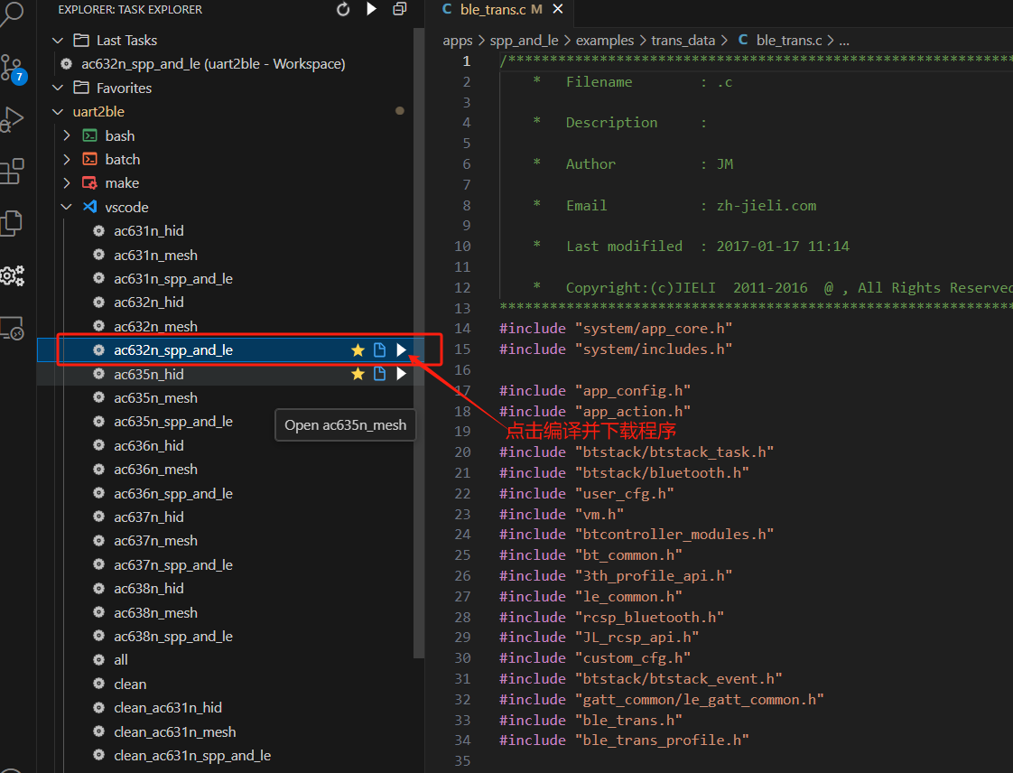
(Click on the image to enlarge it)
You should end up with a message similar to the one below, indicating that the program has finished downloading.

(Click on the image to enlarge it)
- Method 2
If you do not have VS CODE installed on your computer, and do not care about how the source code is implemented, you can download the following attachment "uart2ble_tools.7z", decompress and click on the "download.bat" batch file, you can also quickly download the BLE firmware to the Bluetooth chip.
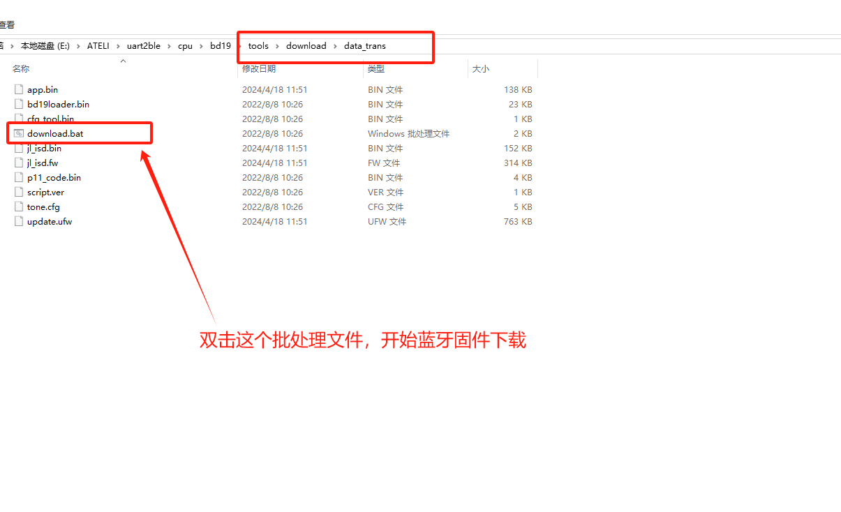
(Click on the image to enlarge it)
After starting the download, there must be the following prompts to be considered successful,

(Click on the image to enlarge it)
- BLE OTA files
1. If you need OTA, the OTA file is in the following directory.
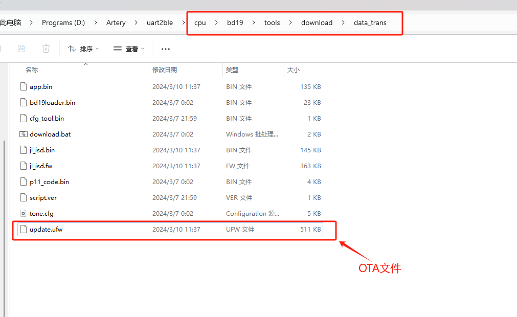
(Click on the image to enlarge it)
Structural components
———————————————————————————————————————————————————————————
The following accessories can be dragged below this link, one-stop collocation of all structural materials, packed, let you worry, let you rest assured, (small partners in need, a lot of support ah! Earn a little money), salted fish: search "USB adjustable power supply structure material package" Finished: Salted fish search "USB adjustable power supply V3 finished product" or station B workshop: Bilibili workshop.
1. 3D Printing shell: 1 pc

2.ABS nylon tube hollow cylindrical straight-through: M4*2.7*4 4pcs

3. Self-tapping screws: M2*12 4pcs

4. Self-tapping screws: M2*6 4pcs

5. Acrylic front cover: 1 piece

6. Acrylic back cover: 1 piece

7. Banana sockets: 2 (1 red, 1 black)
8. Encoder knob cap (15*17MM metal 6MM aperture): 1pc

9. High-side N-MOS heatsink (15*10*20): 1 (not included in the structural material package, must be purchased by yourself)

Other
———————————————————————————————————————————————————————————
1. When the MCU and Bluetooth firmware are successfully downloaded, you need to use a jumper cap to connect the UART of the MCU and Bluetooth, and then the MCU can communicate with the applet.
As shown in the figure below:

Project Current Known Issues!!
———————————————————————————————————————————————————————————
1. In the case of voltage output, adjust the output voltage, and when switching between high voltage and low voltage gear, there is a low voltage output of 2mS.
>>> hardware V4.4 version has been resolved
2024/8/19
2. In the case of no load, after the output voltage, directly unplug the power supply at the input terminal, and there is a problem that the voltage backflow at the output terminal will cause the input terminal (when the voltage is greater than 30V, SC8701 will be basically damaged)
There is a solution to this problem, which requires flying wires and components, as shown in the following figure:
>>> hardware V3.6 has been added to this countermeasure.
3. The voltage is adjusted relatively high, about more than 15V, and the output current limit is less than 2.5A, at this time, the output voltage cannot go up, and the current limit needs to be increased, or the voltage can be adjusted down and the voltage can be slowly increased to output the set voltage normally.
>>> hardware V4.4 version has been resolved
4. If it is a direct short-circuit output, the current limit is not accurate, and it is usually much larger than the set limit current.
>>> hardware V4.4 version has been resolved
5. When the current limit is less than 100mA, the consistency is poor, and the error range between each unit is inconsistent, (it may be that the small signal is easy to be interfered with, the component error, or the accuracy, etc., this problem is left to everyone to fix!!) )
6. It is in the state of current restriction for a long time, and the heat of the high-side current limiting MOS tube is serious, (due to space limitations, it is difficult to achieve ideal heat dissipation of the MOS tube, and it is necessary to pay attention to the actual use scenario during use!!) )
7. The EC11 knob part of the shell, the center position of the opening and the knob needs to be fine-tuned, due to the printing accuracy, the error size of the knob cap, etc., the spacing of the knob cap is not enough, and the hole needs to be increased (you can make do with it for the time being, and then adjust and verify it when you have time)
Everyone is ready to start reproducing, V4.4 is almost perfect!
If you think this project is good, please give it a thumbs up.
At the same time, if you feel that this project has practical value, you are also welcome to click on the collection.
LCD specification: 2.0 inch TFT display 240X320 driver ST7789 interface SPI full color
12Pin soldered LCD
Performance parameters
———————————————————————————————————————————————————————————
1. Input 20V, output 2V, load 4R; Measured wave: 29mV Vpp

2. Input 20V, output 3.3V, load 4R; Measured wave: 40mV Vpp

3. Input 20V, output 5V, load 4R; Measured wave: 50mV Vpp

4. Input 20V, output 9V, load 4R; Measured wave: 56mV Vpp

5. Input 20V, output 12V, load 4R; Measured wave: 68mV Vpp

6. Input 20V, output 15V, load 8R; Measured wave: 63mV Vpp

7. Input 20V, output 20V, load 8R; Measured wave: 78mV Vpp

8. Input 20V, output 24V, load 8R; Measured wave: xxmV Vpp
-----
9. Input 20V, output 34V, load 8R; Measured wave: xxmV Vpp
-----
Other Accessories
———————————————————————————————————————————————————————————
MCU source code address: MCU gitc repository
BLE source code address: AC6328 Git repository
Instructions for the attached files uploaded below:
AT32F421F8P7-USB-PS-V3-V2.1-for-HW4.4.hex: MCU firmware for hardware V4.4
AT32F421F8P7-USB-PS-V3-V2.3-for-HWV4.4.hex: Applicable to V4.4 hardware, optimize and improve the screen refresh rate on the basis of the double buffer DMA algorithm of the little friend "Yinqiao poetry listen", and the current curve has no obvious flash screen phenomenon.
AT32F421F8P7-USB-PS-V3-V2.4-for-HWV4.4.hex: Updated a set of bold fonts for the "Tim" boss.
AT32F421F8P7-USB-PS-V3-V2.6-for-HW4.4.hex: Refactored UI interface, added capacity statistics, temperature display, divided into two interfaces, switch between the main page and the voltage and current page. The following is the demonstration video of Bilibili.
AT32F421F8P7-USB-PS-V3-V2.8-for-HW4.7.hex:only compatible with the hardware version V4.7
[V4.7 software and hardware updated!!] https://www.bilibili.com/video/BV1FBzYYeEat/?share_source=copy_web&vd_source=e41a5e37fca9bfcd8ffac2f41437aa43
AT32F421F8P7-USB-PS-V3-V3.0-for-HW4.7.hex: Only compatible with hardware version V4.7,
1. Optimize the output current limiting mechanism, and fix the serious problem point of NMOS heating caused by device error.
2. Optimize the judgment mechanism of CC and CV.
uart2ble_tools.7z: Bluetooth firmware and download tool
UP_SHELL.stp: Acrylic 3D back cover drawing
DW_SHELL.stp: Acrylic 3D front cover drawing
3D_PRINT_SHELL_2MM.stp: 3D printed shell
If you need it, you can join the QQ group: 594614521
Material Package: Salted Fish Search "USB Adjustable Power Supply Structure Material Package"
Finished product: Salted fish search "USB adjustable power supply V3 finished product" or B station workshop: Bilibili workshop
- The complete production process and demonstration operation of Bilibili:

Video presentation
———————————————————————————————————————————————————————————
- The complete production process and operation demonstration of station B: USB adjustable power supply V3 complete review and production
- Hardware V4.7 Function Complete: Demonstration: [V4.7 Hardware Function Complete Demonstration].
Designed by 黑马小乌龟 (from OSHWHub)
Design Drawing
 The preview image was not generated, please save it again in the editor.
 Empty
Empty


Comment