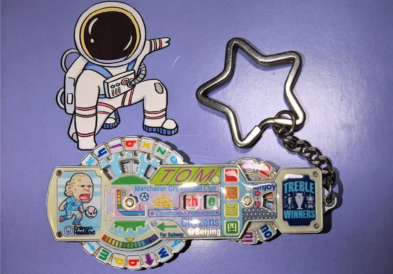
 Completed
Unzipper Keychain _ Manchester City Element _ De Braunay _ Haaland cartoon head
PRO Unzipper Keychain _ Manchester City Element _ De Braunay _ Haaland cartoon head
License
:CC BY-NC-ND 3.0
Description
 Unzip the keychain_Manchester City elements_De Bruyne_Haaland comic avatar.
Features:
1. With NFC coil, it can be used for bus card and access control according to different chips
2. Frontal rotation pinyin combination, Haaland comic avatar, Manchester City triple crown icon
3. The reverse side rotates the pinyin combination, De Bruyne's comic avatar, and the Manchester City football team logo


Design Steps:
1. Use CAD or UG to design the shape, top and bottom rotating shape
2. Import the external dimensions to AD or Jialichuang EDA for PCB design
3. Draw color pictures according to the shape, top and bottom circular rotation shapes
4. In JLC EDA, the PCB is imported with color silkscreen.
Assembly Steps:
1. Use a soldering iron to solder the desired NFC chip to the circular initial rotating plate.
2. Seal the four circuit boards with hard glue to avoid the color silk screen being worn.
3. Solder the two circular PCB centers to the rotating shaft.
4. Install the top, middle and bottom PCBs after sealing according to the positioning holes.
5. The supporting PCB of the middle layer is connected with a key chain.
https://www.bilibili.com/video/BV1NAtZeNEQJ/?spm_id_from=333.999.0.0
Designed by mytom520 (from OSHWHub)
Link:https://oshwhub.com/mytom520/unzip-keychain-manchester-city-elements-de-brauneharland-comic-avatar
Design Drawing
 The preview image was not generated, please save it again in the editor.
 Empty
Empty


Comment