

 Completed
[ Training project ]51 MCU core board
PRO [ Training project ]51 MCU core board
License
:Public Domain
Description
1. Project Introduction
STC89C52RC single-chip microcomputer as the veteran of the 8-bit 8051 series, with its good electrical characteristics and price has been occupying the 8-bit single-chip microcomputer market, as a novice to learn embedded development is a very good choice, itself IO pins are rich, timer, Serial ports, interrupts, ADCs and other peripherals are also complete, and the code of direct operation of registers can help students have a deeper understanding of the working principle of single-chip microcomputer, which is very helpful for embedded learning.
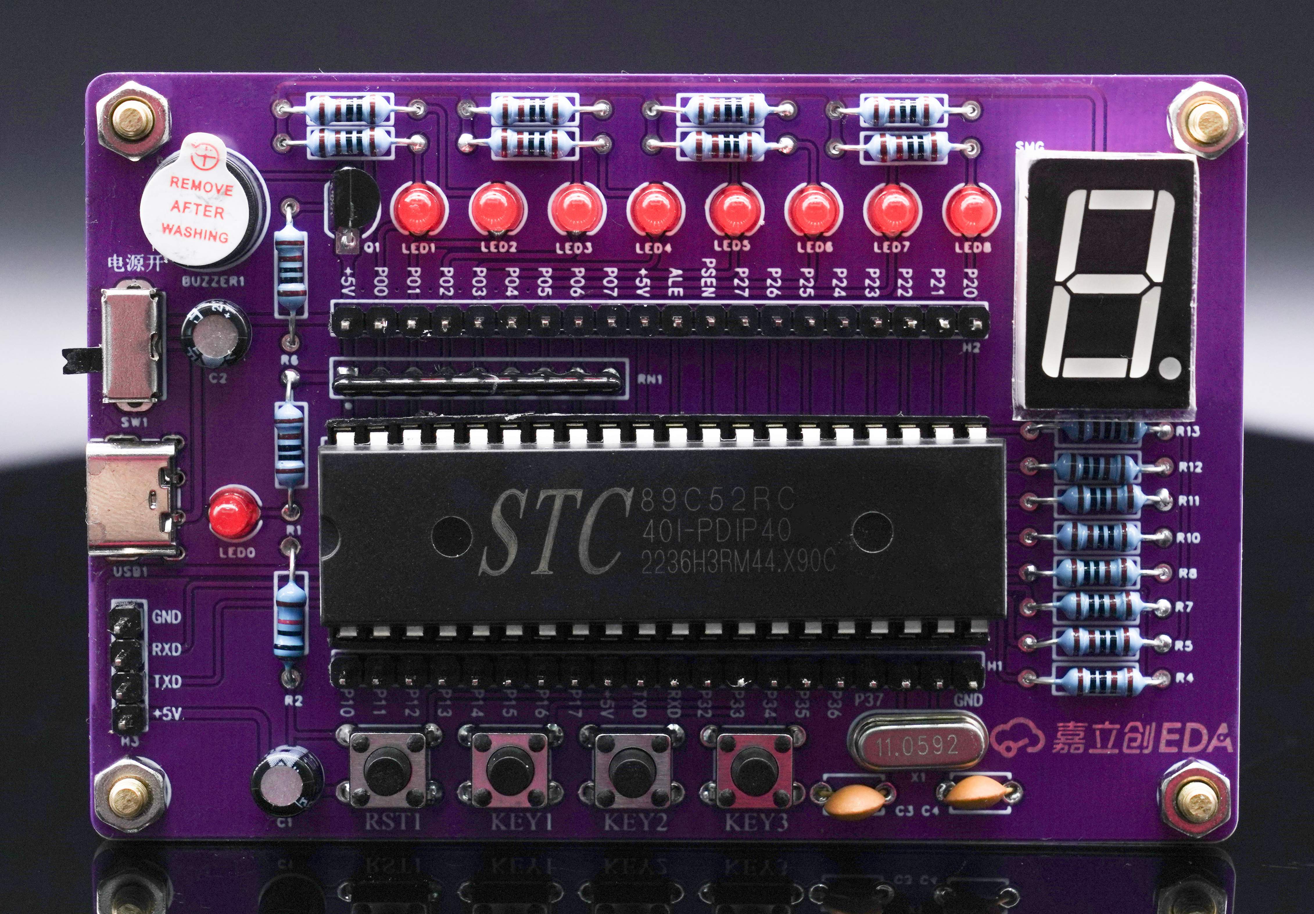
2. Onboard resources

- Main control chip: STC89C5RC-DIP40
- Power interface: TYPE-C-2P
- Peripherals: 8 LED lights, 5V active buzzer, 3 function buttons, single common anode digital tube
- Interface: 2.54*4P download and debugging interface, 2.54*20 expansion pin header interface
3. Advantages and characteristics

- Abundant onboard resources, complete basic peripherals.
- The whole is full of plug-in devices, which is easy to solder.
- Cheap and cost-effective.
- The use of JLC high-quality PCB and Lichuang mall genuine components to ensure product quality.
4. Circuit analysis

Fig.4-1 SCH_51 core board of a microcontroller
1. Power circuit
The power supply circuit is mainly composed of TYPE-C interface, slide switch, filter capacitor and power indicator, using 2Pin TYPE-C interface, simple and convenient, easy to weld, control the conduction and shutdown of the power supply of the whole system through SW1 slide switch, C1 as the power filter capacitor, R1, LED1 form the power indicator circuit, when the system is powered on, the power indicator light is lit to prompt.

Fig.4-2 TYPE-C power supply circuit
2. Main control circuit
The main control single-chip microcomputer uses STC89C52RC (DIP-40 package), the working voltage is 3.3~5.5V, the working frequency range is 0~40MHz, which is equivalent to the 0~80MHz of ordinary 8051, the actual working frequency can reach 48MHz, the Flash program memory space size is 8K bytes, it can be erased more than 100,000 times, the chip integrates 512 bytes of RAM data memory, and the working temperature range is -40~85 °C.

Fig.4-3 Comparison of master control chips
The STC89C51RC/RD+ series is available in HD and 90C versions, which can be distinguished by the last few letters of the bottom line of the text on the surface of the microcontroller.
The HD version does not have P4.4/P4.5/P4.6 ports, and there are 45~100K pull-down resistors inside the RESET pin, and the EA# pin has been pulled up to VCC. The 90C version does not have EA or PSEN pins, and has P4.4/P4.5/P4.6 ports, the ALE/P4.5 pins are used as ALE pins by default, and when used as P4.5 ports, they need to be set in the STC-ISP programmer when burning user programs.
Table 1-1 Definition and reuse of pins on the STC89C52RC core board
| Pins | illustrate |
|
P0.0~P0.7,P1.0~P1.7 P2.0~P2.7,P3.0~P3.7 |
Standard I/O ports |
| RXD | Serial port 1 data receiver |
| TXD | Serial port 1: data transmitter |
| T0/T1/T2 | External input to the timer/counter |
| T2EX | Timer/Counter 2 Trigger control for capture/reload mode |
| INT# | External interrupts, falling edge interrupts, or low-level interrupts |
| WR# | External data memory writes pulses |
| RD# | External data memory reads pulses |
STC89C52RC The P0 port can be used as an I/O port or as an address/data multiplexing bus. The P0 port is an open-drain output, and when used for bus expansion, there is no need to add a pull resistor. When used as an I/O port, an external pull-up resistor of 4.7K~10K must be connected. Here, the P0 port uses a 10K pull-up row resistor--RN1.

Fig.4-4 STC89C52RC main control circuit
3. Crystal oscillator circuit
As the heart of the main control circuit, the crystal oscillator provides a stable clock source for the main control circuit and drives the code to run stably and accurately. The frequency of the crystal oscillator is described according to the official data sheet, it can support 4M~48M, different frequencies, different brands of crystal oscillators, and the load capacitance is not the same, which needs to be selected according to the actual situation, in general, the load capacitance of the 12M~25M crystal oscillator is more suitable to choose about 22~47PF.

Fig.4-5 Crystal oscillator circuit
4. Reset circuit
STC89C52RC is that the high level enters the reset mode, the low level works normally, the reset circuit is analyzed, as soon as it is powered on, the RST button is not pressed, at this time, +5V is given to C2Capacitor charging, capacitor is equivalent to wire, RST is high, the system resets, as the capacitor is close to full, the potential is constant with +5V, at this time no current flows, RST is pulled down to GND by R5to enter normal working mode. If you manually press the RST reset button, at this time, the capacitor will be discharged, even if the capacitor discharge is completed, +5V will flow through the button to the RST, the RST high level will enter the reset button, and when the button is released, there is a process of returning to the previous one.

Fig.4-6 Reset circuit
5. LED display circuit
LED flow lamp circuit, LED lamp is essentially a light-emitting diode, at the positive pole of the diode, add +5V voltage, because the diode resistance is small, if it is directly energized, the flow current will be very large, easy to burn out the diode, joinThe 1K current-limiting resistor limits the amount of current. On the right side of the LED light, connect the IO pin of the STC89C52 microcontroller, when the control IO pin is high, the level of both sides is the same, and the current cannot flow through the light-emitting diode, when the control IOWhen the pin is low, the current flows through the current limiting resistor through the diode to the IO pin to access the GND, and the LED light is lit.

Fig.4-7 LED display circuit
6. Digital tube display circuit
The digital tube is simple to understand, even if there are 7 long LED tubes + 1 round LED light, there is a front LEDThe basis of the running light circuit, the digital tube circuit is very convenient to understand, the digital tube is a common anode digital tube.
Common anode: The positive pole of 8 LED lamps is connected together and led out, and the negative pole of each lamp is controlled separately.
Common cathode: The negative pole of 8 LED lamps is connected together and led out, and the positive pole of each lamp is controlled separately.

Fig.4-8 Digital tube display circuit
7. Buzzer circuit
Buzzers are divided into active buzzers and passive buzzers, active does not refer to the power supply, but refers to the source of vibration, and the buzzer is made by oscillation. The active buzzer used here is the buzzer, which chirps when a power source is given. The buzzer tweets a large amount of current, if the IO pin output high level of the single-chip microcomputer is used to supply power to the buzzer, it may not be enough to make the buzzer call, at this time, add the 8050NPN triode as a control, and control the conduction and closure of the triode by controlling the base current to control whether the buzzer is chirping.
Note: The internal oscillation source of the active buzzer is fixed, and the sound is fixed. The passive buzzer oscillates through an external PWM signal, and the timbre can be changed by changing the PWM frequency.

Fig.4-9 Buzzer circuit
8. Button circuit
Independent key circuit, one side of the key is keyed into the single-chip microcomputer IO pin, and the other side is connected to GND, note that at this time, the single-chip microcomputer IO pin has a lot of output signals, but receives signals, when the other end of the external button is connected to GND, you can enable the internal IO pin pull-up mode, the default pin is high, if the key is pressed, the pin will be connected to GND, and then it is low, so you can check whether the button is pressed by checking whether the corresponding IO pin is low. If one side of the external button is connected to a high level, the reverse analysis can be done, and attention should be paid to increasing the current limiting resistor to prevent the IO pin from being damaged.
Note: After STC89C52RC reset, the IO pin is in weak pull-up mode.

Fig.4-10 Key circuit
9. Interface circuits
The design of this STC89C52RC project, only the IO pins of the single-chip microcomputer are used for learning, embedded is a very large system, and not only the above, in order to facilitate the expansion of learning in the future, no need to repeat the drawing board, add 2.54*20PThe pin header interface is convenient for plugging and unplugging DuPont wires for extended connection. At the same time, through the 2.54*4P pin header interface, the download interface and power interface are drawn out for subsequent program download and debugging.

Fig.4-11 Interface circuit
5. Bill of materials
| BOM_STC89C52 MCU core board | ||||||
| serial number | name | parameter | device designation | quantity | encapsulation | Item number |
| 1 | USB interface | TYPE-C-2P | USB1 | 1 |
USB-C-TH_TYPE-C-31-M-33 |
C2848624 |
| 2 | Slide switches | SS-12D02-VG4 | SW1 | 1 |
SW-TH_SS-12D02-VG4 |
C136719 |
| 3 |
capacitance | 10UF | C1、C2 | 2 |
CAP-TH_BD5.0-P2.00-D0.8-FD |
C43345
|
| capacitance | 47PF | C3、C4 | 2 |
CAP-TH_L4.5-W3.0-P5.00-D1.2 |
C254104
|
|
| 4 |
resistance | 1K | R1、R2~R4、R6~R19 | 18 |
RES-TH_BD2.3-L6.5-P10.50-D0.5 |
C713997
|
| resistance | 10K | R5 | 1 |
RES-TH_BD2.3-L6.5-P10.50-D0.5 |
C410695 |
|
| 5 |
LED lights | red light | LED1、3、5、7、9 | 5 |
LED_TH-3mm |
C99771 |
| LED lights | green light | LED2、4、6、8 | 4 |
LED_TH-3mm |
C85161 |
|
| 6 | Key |
6*6 in-line buttons |
RST1、KEY1~KEY3 |
4 |
SW-TH_4P-L6.0-W6.0-P4.50-LS6.5 |
C393938 |
| 7 | Crystal oscillator |
11.0592Mhz |
X1 |
1 |
HC-49US_L11.5-W4.5-P4.88 |
C358645 |
| 8 | Transistor |
8050 |
Q1 |
1 |
TO-92-3_L4.8-W3.7-P2.54-R |
C3037602 |
| 9 | buzzer |
5V buzzer |
BUZZER1 |
1 |
BUZ-TH_BD9.6-P5.00-D0.7-FD |
C96493 |
| 10 | Digital tubes |
Common anode digital tube |
SMG |
1 |
LED-SEG-TH_10P-L12.7-W19.0-P2.5-S15.24-BL |
C141368 |
| 11 | Pin header |
2.54*4P |
H3 |
1 |
HDR-TH_4P-P2.54-V-M |
C492403 |
| Pin header |
2.54*20P |
H1、H2 |
2 |
HDR-TH_20P-P2.54-V-M-1 |
C50981 |
|
| 12 | Exclusion |
10K |
RN1 |
1 |
RES-ARRAY-TH_9P-P2.54-D1.0 |
C8692 |
| 13 | MCU |
STC89C52RC |
U1 |
1 |
DIP-40_L52.0-W13.7-P2.54-LS15.2-BL |
C14022 |
6. Precautions
When drawing a schematic, you should pay attention to:
- Draw according to the division of module circuits, and indicate the circuit function;
- Fill in the project name and other information on the drawing attributes;
In the purchase of materials, it should be noted that:
- Screen the in-stock materials first, and then filter the price sorting to purchase;
- Try to buy materials from the same warehouse, choose a warehouse close to it, and shorten the delivery time;
- When you purchase multiple orders, you can save shipping costs by binding orders;
In the PCB Layout, it should be noted that:
- The filter capacitor should pay attention to the current flow direction, and try to be as close as possible to the filter element;
- The crystal oscillator should be as close to the chip as possible, and the bottom should not be traced to prevent signal crosstalk;
- The line is preferentially straight, and the place that needs to be turned is mainly obtuse angle or arc;
- Add teardrops after drawing and adjusting the PCB to make the board more beautiful and stable;
- Add silk screen logo and annotate interface functions;
- JLCJLCJLCJLC designated custom silk screen printing can be hidden under the device, and the board is beautiful;

Fig.6-1 Reference diagram of PCB traces - top layer

Fig.6-2 Bottom layer of PCB traces
In welding, attention should be paid to:
- When welding, you can click the welding auxiliary tool in the toolbar of Jialichuang EDA, and the real-time interaction is convenient for welding;
- When soldering the top layer, it is recommended that the main control chip be soldered first to avoid other devices affecting soldering;
- When welding the pin header, it can be used to resist an empty plate or a hole plate to prevent welding skew and affect the use;
- The welding sequence should follow the principle from low to high to avoid affecting the welding of small devices;

Fig.6-3 Empty PCB
During debugging, it should be noted that:
- Before power-on commissioning, check whether there are problems such as virtual welding short circuit in the welding, and check whether the test is correct.
- Use STC-ISP to download programming and programming software, official download address: http://www.stcmcudata.com/
- Use the USB to TTL serial port burning tool to download the program to the single-chip microcomputer, the RXD of the USB to TTL cable is terminated to the TXD end of the single-chip microcomputer, and the TXD is terminated to the RXD end of the single-chip microcomputer;
- After clicking Download/Programming, you need to replug and unplug the VCC to power on, and the handshake operation is successful, that is, the user code has been successfully downloaded.
Designed by 立创EDA课程案例推荐 (from OSHWHub)
Link:https://oshwhub.com/course-examples/dan-pian-ji-51-dan-pian-ji-he-xin-ban
Design Drawing
Intellectual Property Statement & Reproduction Instructions
This is an open-source hardware project. All intellectual property rights belong to the creator. The project is shared on the platform for learning, communication, and research only; any commercial use is prohibited. If your intellectual property rights are infringed on EasyEDA, please notify us by submitting relevant materials in accordance with the Rules for Complaints and Appeals of IPR Infringement.
Users must independently verify the circuit design and suitability when replicating this project. All risks and consequences are borne by the user, and the platform assumes no liability.
 Empty
Empty
Comment