

 Completed
The COM Port Number Visualization Hub
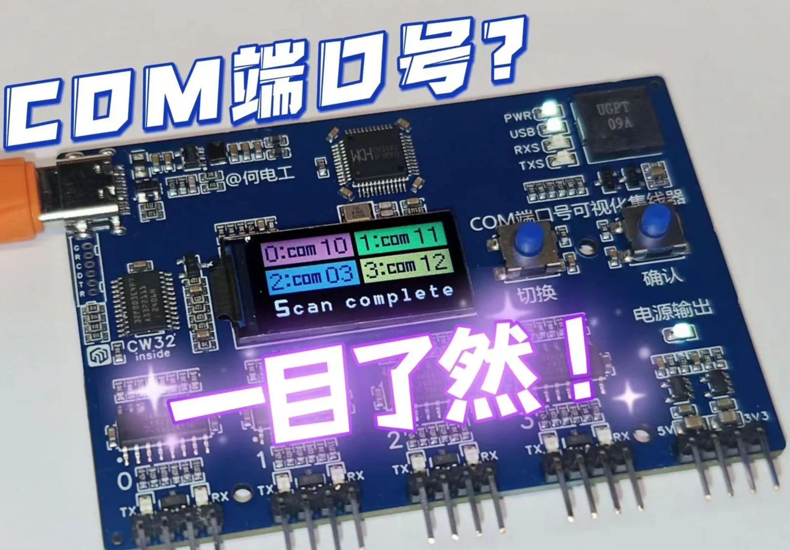
PRO The COM Port Number Visualization Hub
License
:CC BY-NC-SA 4.0
Description
Project Introduction
As a hardware engineer, you often need to use serial ports for data reception, device debugging, etc. When using serial ports to convert USB devices, I believe everyone often encounters a question: "What is the COM number corresponding to this device?" As we all know, this question can The solution is solved by checking the device manager. Although the steps are cumbersome, it is acceptable. However, if multiple serial ports need to be used at the same time, it is not easy to match the COM number with the hardware serial port, which wastes a lot of time before the debugging work begins.
Therefore, this project came into being and adopted the 4to1 serial port HUB+MCU scheme. Just connect the device to the computer, the single chip computer will cooperate with the script of the host computer to scan the serial port, and automatically display the COM port number of the host computer corresponding to the serial port hardware on the device, saving your precious time.
Core Functions
4-way serial port hub, which can convert 4-way ttl serial port through USB.
Display the computer COM port number corresponding to each external serial port.
Promptly remind the user after the computer USB data is abnormally disconnected.
Product Instructions: COM Port Number Visualization Hub Instructions
Project video: [Open Source] Identify the COM port number used in five seconds? I'll help you do it.
Three consecutive + comments to participate in the video debut lottery! (See pinned to the top of the video comment area for details)
Welcome to follow my Bilibili account: @何电工to learn more interesting and practical projects.
This equipment has entered the mass production stage. You can join the communication group to learn about the production progress, and the finished product will be launched.
QQ communication group: 1016193632

Open source agreement
CC BY-NC-SA 4.0
Creative Commons-Attribution-NonCommercial-ShareAlike.
Project properties
This project is made public for the first time and is my original project.
This project has not won any awards in other competitions.
Detailed explanation of hardware
The hardware structure of this project is as follows:
Among them, CH344Q is responsible for the TTL serial port to USB business, and CW32 is responsible for switching the communication path and communicating with the host computer;
The internal power supply of the system is converted from 5V to 3V3 by a DCDC, and the external power supply is from USB5V and outputs 3V3 through LDO.

1. USB to serial port
The core of this project is the CH344Q chip that implements the USB to serial port function. One USB channel can be expanded into 4 serial ports.
The main features of the chip are as follows (screenshot from the chip data sheet):

The peripheral circuit design of the CH344Q chip basically refers to the original factory design, as follows:

The ACT pin of the chip is used to indicate the USB connection status . When the chip is powered but the communication is not successful, it is high level (the R99 pull-up resistor is added here to avoid the instability of the pin level during the chip initialization process and the microcontroller recognition error) , when the chip communication is successful, the ACT pin is low level, and a 10Ω protection resistor is connected to the pin in series to the microcontroller pin to read the USB connection status, so that the buzzer can be used to remind in time when the USB connection error occurs and the disconnection times out. user.
Serial communication rate measurement:
The serial port of this device theoretically supports a maximum of 6M baud rate, and the measured 4 channels can simultaneously carry out normal communication at 460800 baud rate.
2. MCU and peripherals
Considering that this project may need to be used in complex electromagnetic environments such as industrial control/debugging, the CW32 series microcontroller with strong anti-interference ability was selected, and the CW32F003E4P7 single-chip microcomputer was finally selected in combination with the actual needs of the project for the number of IOs, peripherals, and costs.
The debugging interface uses a 1.25 pitch socket, and the debugging interface is the same as my other projects (excluding some projects before 2023), including SWD+UART+RST pins. It is compatible with 1.25/1.27 probe programming without soldering the debugging interface socket, which is convenient for mass production.

This project uses a 0.96-inch TFT color screen, which uses SPI to communicate with the single-chip microcomputer, and uses a digital transistor for screen brightness control, compared with the traditional triode + MOS tube scheme, the peripheral circuit is more concise. In order to reduce the power consumption of the device, it is designed with automatic screen brightness adjustment, which can automatically reduce the screen brightness one minute after the COM port number scanning is completed, and the "dark screen time" can be set by itself, or the automatic screen off function can be turned off.
Other peripherals of the microcontroller also include two buttons and a buzzer.

It should be noted that this project uses a "piezoelectric" passive buzzer, compared to the traditional "electromagnetic" passive buzzer that only needs a triode to drive the sound, the piezoelectric buzzer must be driven by a push-pull circuit to make the piezoelectric ceramics occur based on the reverse piezoelectric effect. Since the volume requirement of this project is not high, a 5V voltage is used to drive the buzzer, and if you want the piezoelectric buzzer to emit a high volume (which is also a characteristic of piezoelectric buzzers), a special drive circuit is required for boost control.
3. Communication path switching circuit
The communication path switching circuit is the core of this project, in order to better understand the implementation logic of this project, we first need to understand two points:
(1) The CW32 main control chip only controls the logic related to "communication path switching", while the "USB to TTL circuit" is controlled by CH344Q, and the two services are independent of each other, so when the "communication path switching circuit" switches the operation, it will not affect the work of the "USB to TTL circuit", so CW32 can use any serial port of CH344Q to communicate with the host computer after switching the path;
(2) The serial slogan of the single-chip microcomputer during scanning is the external serial slogan, so the serial slogan of the CH344Q chip is different from the external serial slogan, which does not affect the scanning and final scanning results, and the modification of the corresponding relationship of the COM number is only to optimize the wiring and avoid winding;

As shown in the figure above, the communication path switching circuit of the four serial ports is exactly the same, and each is free to switch a 4052 "double-pole four-throw" analog switch chip, in which the common end is CH344 one end, that is, the HUB end, and the two channels of 4052 A/B correspond to TX/RX respectively, which is exactly a group of serial ports, and the four ends of the "four throws" are:
00: Status 0, TX and RX are grounded with 200K resistors, and the communication is off. In the early design, the 10K resistor grounding scheme was adopted, and it was found that a set of 00 data would be sent out at the serial port during the 4052 switching, and a large amount of useless data would be sent to the host computer during high-speed scanning, so the 200K resistor was changed to reduce the speed of the level to avoid sending useless data and causing communication interference;
01: State 1, the TX and RX of the current channel are connected to the RX and TX pins of the single-chip microcomputer respectively, so that the single-chip microcomputer can use the "USB to TTL" function of the current channel to communicate with the host computer (computer); (It should be noted that only one set of serial ports can communicate with the serial port of the single-chip microcomputer at any time, otherwise it will cause communication errors or failure to communicate)
10: In state 2, the TX and RX of the current channel are shorted with a 0Ω resistor and are in the internal loopback state. However, since 4052 has on-resistance, there is about 100Ω series resistance between RX and TX in the case of short circuit.
11: Status 3, TX and RX are connected to external interfaces, that is, normal communication mode;
The status control IO of 4052 is A0, A1 is dropped down by default, the MCU can use IO control, the A0 of 4 pieces 4052 is unified control, and A1 can be controlled independently. In this way, we can save IO for state control while ensuring that each serial port can communicate with the single chip computer separately. If you need to make an 8-way serial port hub, you can use the displacement selector chip to poll the A1 and control its level.
4. Power supply
The device has two independent power supplies, one set of 5V-3V DCDC power supply for internal power supply, and the other set of 5V and 3.3V power supply with current limit protection for external power supply.

The external power supply is designed with MT9700 for 300mA current limit protection to prevent damage to the computer when the external device is abnormal or short-circuited. If the external device is overloaded and the protection is triggered, the "Power Out" indicator will turn off for a warning. The USB interface protection current of most computers is 0.5-1A, so even if the external 5V short circuit of this device will not cause USB protection, but the protection threshold of some computers is small, which will cause the USB port to enter the protection mode, in this case, the USB data cable is turned off, you will find that the PWR indicator of the device is on, but the USB indicator is off, at this time the buzzer will alarm, in this case, you need to disconnect the device from the computer and restart the computer, and the USB port can resume normal work.
The external power supply is also designed with LDO to output a 3.3V, which is convenient for users to use when debugging single-chip microcomputers and other equipment. It should be noted that the 3.3VOUT upper power supply is 5VOUT, so it shares the output power limit with 5VOUT, and the overload of either output power supply will trigger protection.
The enable pin of MT9700 is pulled up at 3.3V, and the output enable pin of capacitor charge control is used with a large resistor, so that the output time of the external power supply is later than that of the onboard device.

One of the channels is USB power supply (5V), and the overshoot depends on the power supply equipment (computer) and has nothing to do with this equipment; 2 channels are 3.3V, 3 channels are SCM RST pins, 4 channels are 5VOUT (M9700 output), and the 5VOUT output time is later than the onboard device to ensure that the peripherals are started in order.
5. External Interface
The device uses a 90° row of wires for external connection, using a standard 2.54 pitch, can use Dupont wire, and is also compatible with XH2.54 and other common connection methods.
The interface is equipped with a TVS protection tube to prevent the equipment from being damaged by static electricity when the user touches it, and improve the reliability of the equipment.
Each group of serial ports is provided with independent TX and RX signal indicators, of which TX is green and RX is blue, which is convenient for quickly identifying the communication status. Each set of indicators has its own beads to prevent high-frequency interference from coupling to the power line during high-speed communication.

As shown in the figure above, the middle two pins of each group of 4P headers are TX and RX, while the two pins on the outside are GND
In this way, the design of GND pins on both sides is to be compatible with different line sequences and improve the user experience.
The pin function is printed on the back of the module: G=GND, T=TX, R=RX.
Software In Detail
This project is written based on the standard library, because the main control chip Flash is small, bare metal programming is used, and only the necessary files are imported, so as to reduce the program size. The core business logic and other key codes involved in this project are described below.
Note: The code of the lower computer of this project is completely open source, and you can download the "ComHubProject.zip" file in the attachment, and the code is annotated in detail for easy understanding.
1. Master-slave Interaction
The core of this project is to detect the COM number corresponding to the slave CH344 chip by sending the COM number of the computer through the host.
The master-slave node establishes a TCP connection and then checks the COM number through UDP. The detailed process is as follows:
(1)TCP
The first handshake: It will be automatically initialized after the slave is powered on, and will continue to send requests to the host to determine whether the host is online. This step ensures that the slave is aware of the status of the master, preventing the slave from wasting resources when the master is offline.
The second handshake: After receiving the slave's request, the master responds to the slave's request and informs the slave that the master is now online and can enter the COM port scanning stage at any time. This step confirms the connection between the master and slave, ensuring that the slave does not move on to the next stage until the master is ready.
The third handshake: After receiving the response from the host, the slave will first close the receiving interrupt of the serial port, and then send a confirmation message to the host, indicating that the slave is ready to enter the COM port scanning stage. Turning off receive interrupts prevents other extraneous signals from being received at this stage, thus avoiding interference.
(2)UDP
After entering the COM port scanning stage, the communication mode of the master and slave is switched to UDP, so that the efficiency of UDP can be used to quickly transmit data. The host continuously sends the information of the four COM ports corresponding to the CH344 chip through polling, and the slave uses the timeout mechanism to determine the COM ports of the computer corresponding to these four channels.
(3) Communication protocols
| FH | DL | FC | Data | CRC8 Checksum | FD | |
| The slave sends a COM port detection request | B5 | 02 | 01 | 00 | XX | 5B |
| Host response | A5 | 02 | 01 | 00 | XX | 5A |
| Slave response | B5 | 02 | 02 | 00 | XX | 5B |
| The host polls to detect the COM port | A5 | 02 | 02 | The com port number on the PC | XX | 5A |
| The slave sends a communication stop signal | B5 | 02 | 03 | 00 | XX | 5B |
Although the content of the communication required in this project is relatively simple, it is still necessary to use the standard communication format, which is due to the fact that when the serial port polls for receiving/transmitting, the analog switch will be used to connect the unused three-way serial port to ground, which will cause the RX signal line to have a falling edge signal, from the probability of sending a "useless" byte to the host computer by mistake, and if the communication protocol is not used, this useless byte will be accepted by the host computer and affect the normal communication.

(4)Q&A:
(1) Why do you need to use TCP and UDP at the same time?
TCP reliability: At the beginning of the master-slave connection, both parties need to confirm that the other is online and ready to communicate. TCP provides a reliable connection, ensuring data integrity and transmission sequence. It is very important to establish a stable TCP connection before communication begins to avoid data loss and misjudgment.
UDP efficiency: In the COM port detection phase, the communication requirements are fast and stateless. UDP is lighter than TCP and doesn't have a complicated handshake process, which makes it ideal for sending and receiving data quickly in a short amount of time. Since UDP does not have a retransmission mechanism, it is more suitable for scenarios where even packet loss does not affect the overall operation, such as in COM port scanning, the master constantly polls and sends data, while the slave only needs to receive data.
In summary, the use of different communication protocols at different stages of the project can take full advantage of the best of both worlds: TCP for reliable connections and UDP for efficient data transmission.
(2) Why not use a two-way handshake?
Risk of a two-handshake: In the case of a two-handshake, the host may start scanning the COM port before the slave is fully ready. This results in the host's scan data not being received correctly by the slave, which in turn leads to data misjudgment. With the third confirmation of the three-way handshake, the slave can explicitly notify the master that it is ready for COM port scanning, avoiding the problem of state out-of-sync between the master and the slave.
Slave state switching: The slave may be working on other tasks at the time of the first handshake, such as polling multiple channels. In this case, if you directly enter the COM port for scanning, the status of the slave may not be switched in time, further increasing the risk of false positive.
The three-way handshake design ensures that the master and slave start the COM port scan in the same state, avoiding potential synchronization problems and false positives.
(3) Why not solve the problem with a delay?
Uncertainty of time: In embedded systems, it is very difficult to synchronize time between different devices. Even if the host enters the COM port scanning mode with a response delay, there is no guarantee that the slave enters the scanning mode within the same time window. This uncertainty in time can lead to synchronization problems between master and slave, which in turn can lead to communication errors.
Timeout mechanism of the slave: The timeout error counting mechanism is used in the COM port detection of the slave. If the slave enters scan mode earlier than the master, the timeout mechanism may be triggered by waiting for the host's data, resulting in a false judgment of the slave.
Therefore, a time-dependent approach cannot guarantee reliable communication, in contrast, a design that uses a three-way handshake can more precisely control the state synchronization of the master-slave device and ensure reliable communication.
Summary: The design scheme makes full use of the reliability of TCP and the efficiency of UDP, and ensures the state synchronization and data transmission accuracy of the master-slave device through the three-way handshake mechanism. This design is reasonable and necessary to avoid misjudgments and communication errors.
2. Serial Port Timeout Reception
In serial communication, timeout reception is an effective method to deal with incomplete data reception. There are two common application scenarios:
(1) Fixed-length data: If the sender fails to complete the transmission of a frame of data for some reason, the receiver needs to judge whether the data is complete through the timeout mechanism to avoid wasting system resources. The receiver sets a timeout value, and if no more data is received within this time, the current data frame is considered to have been received.
(2) Indefinite length data: If the data length is not fixed and there is no clear frame end, it is difficult for the receiver to judge whether the data is received completely. Through the timeout mechanism, the receiver can monitor the change in the length of the data, and if the length of the data remains the same for a certain period of time, the data receipt is considered complete.
In this project, we experimented with the use of software timers and hardware timers with flags. The experimental results show that the combination effect of hardware timer and flag bit is better, which indicates that the serial port timeout reception has high requirements for accuracy. Let's take a look at a few of the timing mechanisms that are commonly used in projects.
3. Timing Mechanism
(1) Software timer: The software timer relies on the time base unit provided by the hardware timer, such as the tick timer. It manages scheduled tasks on the basis of system scheduling, and although it has high accuracy, it may have a slight scheduling delay due to the system load. The implementation of the software timer can be achieved by adding 1 to the global variable every time an interrupt is generated in the hardware timer, and judging whether the timer time has been reached by comparing the last count value with the current count value in the main program. However, this method is cumbersome and requires a flag for each scheduled task. To simplify timer management, MultiTimer v2 can be used, which provides more elegant timer task management by sorting linked lists by timeout times. For more information about the migration process, please refer to the link [MultiTimer v2 Migration Process].
(2) Hardware timer and flag: The combination of hardware timer and marker can significantly improve the timing accuracy. The timer generates an interrupt and changes the global flag, and the main program detects the change of the marker and performs the corresponding operation. This method has high accuracy and is suitable for applications with strict timing requirements, such as the serial port timeout reception in this project.
(3) Hardware timer output capture function: Hardware timer output capture is used for high-precision timing tasks, which can be accurate to the microsecond level. When an output capture interrupt is triggered, the corresponding callback function is executed immediately. Despite the high accuracy, the first two timing mechanisms were used to meet the timing requirements due to resource constraints.

4. Key Drive Module
In previous projects, I would have implemented my own software debiting schemes based on timers and state machines. However, in order to improve the development efficiency, this time we chose MultiButton, a small, easy-to-use event-driven key driver module. The MultiButton module manages key input in an event-driven manner, automatically handling debounce and multi-button combinations.
Compared to traditional state machine-based software debounce schemes, this modular design simplifies code structure, reduces debugging time, and significantly improves system flexibility and reliability. Since the MultiButton module has a built-in mature debounce algorithm and key event handling mechanism, developers no longer need to write complex code for these basic functions, so they can focus more on the core logic development of the project.。
For more information on the migration process of the MultiButton module, please refer to the following link: [MultiButton Migration Process].

5. UI interaction
The UI display in this project plays a core function, and every time the user uses the device, the final thing is to understand the COM number by looking at the screen, so the UI of this project has been optimized in a key way, especially the font library and display part.
On the surface, this project uses 1608 and 2412 fonts, but in fact, these two fonts have undergone special treatment, so this project actually includes 5 sets of fonts: 1608 special fonts (including only the three letters "C, O, M"), 2412 NUMERIC FONTS, 2412 UPPERCASE FONTS, 2412 LOWERCASE FONTS, and 2412 SYMBOL FONTS, all of which are modeled from different computer fonts.
Among them, the font of the three special symbols of "#¥%" in the 1608 special font library is replaced by the font corresponding to the "COM", and the remaining part of the font is deleted to solve the flash space.

Because the single-chip microcomputer uses an isometric font, when displaying a particularly thin font such as i or lowercase L, and when displaying a particularly wide font such as M or W, it may cause a poor overall appearance, and it should be noted that in the case of mixed display of case and English numbers, some fine-tuning is needed to obtain a better display effect, so the code of the UI display part of this project is more complicated.

The image above shows a screenshot of some of the code displayed in the UI, which shows the fine-tuning of some character positions.
Note: This project is my first time to do a font library, because I didn't find a systematic tutorial, mainly I groped and tried to do it many times, the font library is not very good, so I need to fine-tune it in the UI code, and the follow-up project will remake a set of font libraries for easy use. After the font library is proficient, we will consider making a set of non-monospaced fonts to get the best display effect.
Easter eggs: The UI color scheme of this project refers to the color scheme of internationally renowned manufacturers, and friends who find it can write in the comment area.
6. Host (upper computer) Detection
The host computer is written based on Python, and the exe file has been generated, please download it in the attachment.
The core logic of the host computer revolves around the detection, configuration and communication of serial port devices. The host computer program will scan all serial devices in the system for serial ports that contain the specified string (currently set to "CH344") in the description information. If a matching serial port is found, the program will check whether the manufacturers of these serial ports are consistent to ensure compatibility between devices and reliable communication.


After finding the serial port that meets the requirements, the program configures the communication parameters and enters the loop of polling the communication. The host waits for the slave to send a request signal (function code is 0x01), and after receiving the request signal, it sends a response frame and clears the receive buffer of the serial port. Next, the host waits for the slave to send a startup signal (function code 0x02). When the boot signal arrives, the host begins polling communication between the four serial ports.


During the polling process, each serial port sends a data frame containing the function code and port number in turn, and the other serial ports receive the data and verify its validity. If the received frame contains a stop signal (function code 0x03), the communication is terminated and the program exits. During the whole process, the CRC8 verification algorithm ensures the integrity of the data.
This logical design enables the program to effectively manage the communication between multiple serial devices, ensuring the accuracy and consistency of data transmission.
Project Fork Considerations
1. The shell file can be recommended for 3D printing, and the upper panel is recommended to be processed by acrylic laser cutting, and the thickness of acrylic is 1.8mm. The 3D files and acrylic cutting DXF files required for the project are all attached to the project, please download them by yourself. Note: Many Taobao stores mark 2mm acrylic, and the actual thickness is 1.8-1.9mm, please contact customer service for confirmation.
2. When the project is reproduced, it is recommended to use the probe to burn, if the debugging socket is welded, it needs to be removed before installing the equipment shell, and the plastic shell of the socket can be pulled out with needle-nose pliers first, and then the connecting pins can be removed or cut off one by one, otherwise the debugging interface socket will interfere with the acrylic on the upper panel.
3. Procurement links for special components and structural parts, please pay attention to the specifications: (non-advertising, for reference only)
Silicone button Category: 5.2H Note: The "TS-1158UB-C-D-BL" button with a height of 5mm was selected in the project, because the highest silicone button in the JLC mall is this model, and it is recommended to use 5.2 or 5.5 head high for a better feel when reproducing it by yourself
0.96TFT display Category: BOE welded glue iron integration
M2 Support Copper Pillar Classification: M2*2.5*3
Top plate small head screw Classification: M2*3.5*3 head diameter
Base plate countersunk screws Classification: M2*5 blackened
4. There are six round holes on the PCB, three of which are M2 screw fixing holes with a diameter of 2.1mm, and two of the diagonal of the PCB are 1.152mm special positioning holes for economic SMT.

Other
The CH344Q chip used in this project natively supports RS232/485, if you don't have the need for a TTL serial port at all, you can directly modify the motherboard to support 232/485 communication without using an expansion board.
Based on the current version of hardware and software, a computer can only connect to one visual serial hub. In the future, if there are more people who demand "more serial ports", there may be a version of USB to 8 serial ports (Gugugu), welcome to add a group to urge the update.
If you have any questions or suggestions about the project or the reproduction process, please join my chat group!
QQ group: 1016193632

Project Video: [Open Source] Identify the COM port number used in five seconds? I'll help you do it
Triple + comment to participate in the video launch raffle! (See the top of the video comment section for details).
Thanks
Special thanks to the JLC open source hardware platform and the CW32 ecological community for their support to this project!
Special thanks to aiapp-isp software, very easy to use font editing software!
Special thanks to the following friends for their help and contributions to this project:
Software: @C_P
Image: @耿先生工作室
Test: @琴弦
Thank you again for answering my questions during the project design and commissioning!
Designed by 何电工 (from OSHWHub)
Link:https://oshwhub.com/heyh/comportnumber-visualization-hub
Design Drawing
Intellectual Property Statement & Reproduction Instructions
This is an open-source hardware project. All intellectual property rights belong to the creator. The project is shared on the platform for learning, communication, and research only; any commercial use is prohibited. If your intellectual property rights are infringed on EasyEDA, please notify us by submitting relevant materials in accordance with the Rules for Complaints and Appeals of IPR Infringement.
Users must independently verify the circuit design and suitability when replicating this project. All risks and consequences are borne by the user, and the platform assumes no liability.
 Empty
Empty
Comment