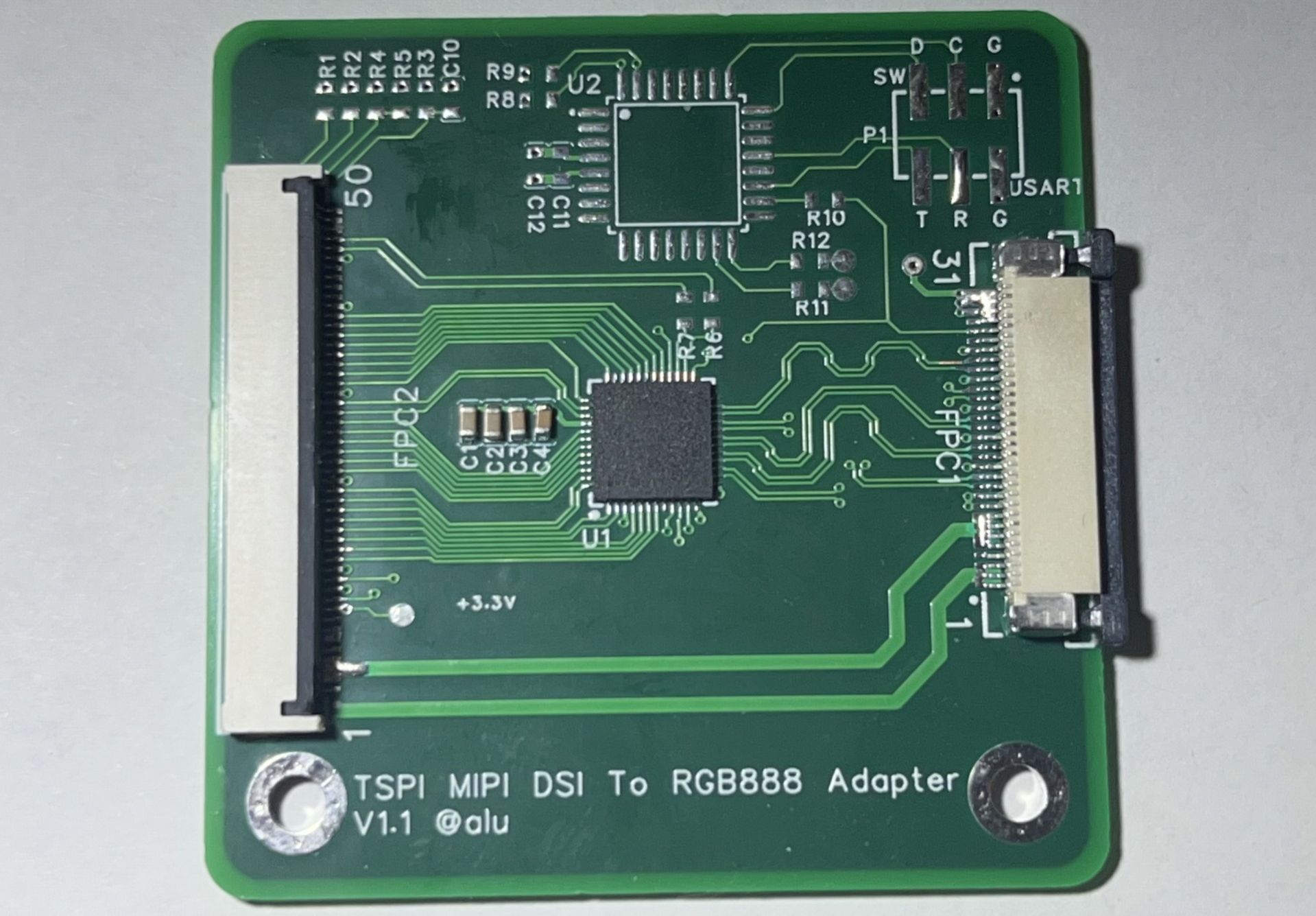
This project is open source and shared in its current state without warranties of any kind, either express or implied.
The use of this open source project requires considerable knowledge of electronic software and hardware, and whether there is any risk at your own discretion, and the author is not responsible for the consequences of personal injury and damage caused by the use of this project.
If you do not agree with the above information, please close this page immediately, and if you do, please continue reading.
**This document only explains the content closely related to this project, please refer to their respective documents for other related knowledge.** This document is based on the Tarzanpai/Rockchip SDK's buildroot toolset, and other systems such as Ubuntu are not tested, but should work universally. This document does not explain in detail how to use Tarzanpai/Rockchip SDK/Linux Device Tree/STM32. This project is only suitable for the MIPI interface of the Taishan Pai development board and the FPC line sequence of the LCD screen for testing, and needs to match the MIPI interface and other LCD screens of other development boards, and you need to modify the line sequence in the project, design the adapter board or use the finished adapter board to transfer the FPC line sequence, etc., see the hardware section below for the transfer method. This project does not involve the touch part, if you need a touch function, please refer to the Taishan Pai document to use the touch interface of Taishan Pai. In the following, MIPI Rate, Lane Rate, and MIPI Lane Rate all refer to the same data, but in different terms.
# The hardware part ICN6211 the conversion chip and the STM32 debug chip
###### The circuit board only needs to be soldered at least ICN6211, 4 capacitors and FPC connectors on the MIPI side and RGB side can be used, if you need to further study ICN6211, you can solder STM32 and related resistance capacitance, 6pin connectors, etc., and use STM32's I2C interface to initialize and debug the ICN6211.
###### Under the simplest configuration, the cost is only 7.6 yuan, which greatly expands the range of screens that can be used by Taishan pie.
######
###### ICN6211 ¥5
###### 4pcs 0603 capacitor ¥0.1
###### 2 FPC connectors ¥2.5
###### Total ¥7.6
###### If you need to add STM32G030K8T6 for debugging and initialization, you need an additional 3 yuan.
### Directions of use:
##### 1. Taishanpai's MIPI DSI interface has provided an LCD backlight power supply, please pay attention to the positive and negative poles when using this power supply, reverse connection may damage the device.
##### 2. The default configuration current of Taishan Pi MIPI DSI interface backlight driver is constant current of 111 mA, please pay attention to the working current of the LCD screen used, if the working current of the LCD screen is much less than 111 mA, there are two ways to adjust:
###### 2.1 Method 1: Adjust the R95 and R96 resistors of Taishanpai, remove one resistor to reduce the backlight current to 55.5 mA, or read the SY7201ABC backlight driver chip document carefully and select the appropriate current configuration resistor according to the 200mV feedback voltage.
###### 2.2 Method 2: In the device tree file tspi-rk3566-dsi-v10.dtsi mentioned in the software section, reduce the backlight PWM and the output current is roughly 111 * PWM / 255 (mA), Method 2 is not verified, please use it with caution.
##### 3. If you use an LCD screen with a backlight driver board installed, you need to draw a 5V power supply VCC5V0_SYS (or the power supply required by the LCD driver board) from the 40Pin expansion header on Taishan, instead of using the backlight power supply provided by the MIPI DSI interface on Taishanpi
##### 4. Minimal configuration of the components required for soldering:
```
U1,
C1, C2, C3, C4
FPC1, FPC2
```
##### 5. C13, C14, C15, C16, C17, C18 are decoupling capacitors designed for ICN6211 VDD1-VDD3, which are not mentioned in the documents that can be searched in ICN6211, and after preliminary testing, they can work without soldering these capacitors ICN6211
###### C1, C2, C3, C4 are connected to the LDOs inside the ICN6211 that power the cores, and ICN6211 documentation clearly states that they must be there, at least two capacitors, 1uF + 10nF.
##### 6. The two screw holes correspond to the short-side screw holes of the Taishan faction, which can be connected with the Taishan faction through the copper pillar.
##### 7. The MIPI side connector FPC1 uses a 31pin 0.5mm FPC to connect, if there is a Pin number on the purchased FPC cable, please ignore it, and the Pin number on the board and the schematic diagram shall prevail.
##### 8. RGB side connector FPC2 uses 50 pin 0.5mm FPC to connect up and down, which is convenient for replacing various co-directional and off-direction FPC cables.
##### 9. When using FPC flexible cables, please carefully check the correspondence of the pins, reverse connection may damage the device. Tip: Abandon the concept of the front and back of the FPC soft cable in your mind, and only pay attention to whether Pin1 is connected correctly, regardless of whether it is connected positively or reversely, as long as Pin1 is connected correctly, it will not be wrong. In this project, the Pin1 of the silk screen near the FPC on the PCB of this project is marked as a non-standard Pin1 position, and the order of the Pins is also marked on some FPC lines.
##### 10. If you want to study the functions of the ICN6211 chip in depth, you can refer to EDA engineering to solder STM32, use the I2C interface to communicate with the ICN6211, debug and DEBUG, the project design has reserved USART I2C and some GPIOs for STM32.
###### 11. Most of the current screens have DE signal input, so the VSYNC and HSYNC on the default PCB are disconnected, if needed, solder R6 and R7 resistors.
###### 12. R1, R2, R4, R5 are the configuration resistors of the screen used during the test, all of which can be soldered, and R3 and C10 are the RC networks for the Reset Pin on the screen. The on-screen driver chip of some screens may have requirements for the Reset circuit, such as the need for an RC network to ensure that the Reset signal is stable.
### Runtime photos
![运行图片1.jpg](//image.lceda.cn/pullimage/u167xNwxswcJiBKAxatsbykdy3TbZgVIoslWguFP.jpeg)
### PCB 3D rendering
![3DPCB.PNG](//image.lceda.cn/pullimage/UIO3PNritqXk2J2vuCzAweSJ2IiWxLr0uDgT2S06.png)
### Transfer method
###### For screens with different pins and different line sequences, you can use the following adapter board to transfer, two adapter boards are connected by Dupont wire to adjust the line sequence, which can theoretically drive any RGB screen, and some RGB screens need SPI initialization, and there are two ways to initialize:
```
1. The SPI3 interface is initialized via Taishan's 40Pin extension.
2. Modify the circuit of this project to connect the SPI interface of the STM32 to the 50Pin FPC connector and initialize using the STM32.
```
![FPC_2.54_转接板1.jpg](//image.lceda.cn/pullimage/qnPxL8pYvBHcrm261F1UyP8k8K307TVz4VPGBHVF.jpeg)
### Screens with different wire sequences driven by the adapter board
###### The screen is a screen with a backlit driver board installed, so there are two wires to send 5V and 3.3V power supplies from Taishan to power the driver board.
![FPC_2.54_转接板_亮屏1.jpg](//image.lceda.cn/pullimage/0xMUT9MglOvJscOAUSkwdr4H7z8zUHhiQsTku4O3.jpeg)
###### This method is very cumbersome, and there will be a lot of Dupont lines on the desktop, so if you can, you can still draw the board yourself to change the line order, or make an adapter board, which is more convenient to use.
### Purchase link
###### Except for the ICN6211 and 31pin 0.3mm to 0.5 mm FPC cables, all other devices can be purchased from the LCSC, and you can choose from EDA to place an order with one click.
###### Here are the purchased connections for ICN6211 and 31pin 0.3mm to 0.5 mm FPC cables:
**ICN6211**
[https://item.taobao.com/item.htm?_u=8153gbt7a66&id=748653542037&spm=a1z09.2.0.0.2e502e8dbZVk4x](https://item.taobao.com/item.htm?_u=8153gbt7a66&id=748653542037&spm=a1z09.2.0.0.2e502e8dbZVk4x)
**31pin 0.3mm to 0.5mm FPC cable**
[https://item.taobao.com/item.htm?spm=a1z09.2.0.0.1f212e8dcrxglx&id=639417787070&_u=8153gbtd541](https://item.taobao.com/item.htm?spm=a1z09.2.0.0.1f212e8dcrxglx&id=639417787070&_u=8153gbtd541)
# Software part
ICN6211 Configuration parameter calculation and Linux device tree configuration.
##### Abbreviation:
VFP: Vertical Front Porch
VBP: Vertical Back Porch
HFP: Horizontal Front Porch
HBP: Horizontal Back Porch
### The relationship between MIPI Rate and PCLK
ICN6211 The pixel clock PCLK output to the RGB screen can be obtained from the MIPI CLK through the ICN6211 internal PLL division, or from the REF_CLK pin input to the external clock source.
The pixel clock PCLK of the RGB screen and the MIPI Rate/MIPI CLK of Taishan Pai (MIPI Rate=MIPI CLK*2) need to meet the following conditions 1-4 to display the picture perfectly:
1. The actual MIPI Lane Rate is an integer in MHz;
2. Minimum MIPI Lane Rate = (PCLK * 24) / (Number of MIPI Lanes used), 24 is the number of bits per pixel of RGB 888, that is, the number of clocks that need to hop for each pixel to be displayed in MIPI DSI Lane;
3. Actual MIPI Lane Rate = PCLK * power of some 2;
4. The actual MIPI Lane Rate calculated by 3 is greater than the minimum MIPI Lane Rate and less than the maximum rate calibrated in Rockchip's MIPI DSI specification document (e.g., 1000MHz);
5. When initializing the ICN6211, the MIPI CLK = MPI Rate / 2 filled in the configuration software described below is also how the actual MIPI works, similar to DDR, the rising edge and falling edge are sampled, so the MIPI clock is half of the MIPI Rate, and ICN6211 only samples on a single edge when using the MIPI clock as a reference.;
6. The actual MIPI Lane Rate also needs to meet the settings of the Rockchip SDK driver, which will automatically change the MIPI Rate in the device tree file that is not a multiple of 6 to a multiple of 6, I didn't read the driver code, but I guess it is also the reason for the Rockchip MIPI clock PLL;
7. The reason for this large number of limitations is that when ICN6211 uses MIPI CLK as the reference clock, the PCLK is obtained by the MIPI CLK divider, and the PLL divider of the ICN6211 can only be divided into 2, 4, 8, and 16, so it can only be matched with all other parameters, and the parameters will almost flicker. Originally, the PLL of the ICN6211 supports fractional multiplication/division, but due to the lack of smooth documentation, no configuration method was found, and the open source configuration software does not support setting fractional PLL registers, I guess if the fractional PLL configuration ICN6211 is used correctly, there should be no need for the following 9.1-9.4 like the number;
8. Since my PCLK needs to be around 27MHz, I measured up to 2 Lanes MIPI Rate of 984 Mbps, and the screen was overclocked to a 67Hz refresh rate, but it still displayed normally. In addition, if the device tree of Taishan Rockchip SDK sets the MIPI Rate to exceed 996MHz, it will be automatically reduced to 996, so if the actual MIPI Rate is calculated to be too large, the channel will be doubled (2 to 4), so that the MIPI Rate can be halved, and the MIPI Rate=PCLK * 2 power condition is also met;
9. The above are all theories, and the practical operation of saving the stream is coming:
Since the minimum MIPI Lane Rate = PCLK * 24 / (number of MIPI lanes), the minimum MIPI Rate is basically only 4 numbers in the case of a total of 4 Lanes: PCLK * 24, PCLK * 12, PCLK * 8, PCLK * 6, and on this basis, the actual MIPI Lane Rate that satisfies the conditions of 1-8There are only 3 numbers: PCLK * 32, PCLK * 16, PCLK * 8,
So the simplified calculation is:
### Simplify the calculation method
9.1 For the time being, PCLK will round up near the data given in the screen parameter document, for example, the parameters given by the screen manufacturer are as follows:
```
HActive = 800
VActive = 480
HFP = 36
HSync = 2
HBP = 36
VFP = 20
VSync = 2
VBP = 20
刷新率 = 60Hz
```
Calculate the PCLK first
```
PCLK =
(HActive + HFP + HSync + HBP) * (VActive+VFP+Vsync+VBP) * 60Hz =
(800+36+2+36) * (480+20+2+20) * 60 =
27373680Hz
```
Rounded to PCLK = 27000000Hz = 27MHz, as for why rounding, see 9.3, 9.4.
9.2 Suppose we use 2 MIPI Lanes, we don't need to calculate the minimum MIPI Lane Rate, we can directly calculate the PCLK * 16 or 32 above to get the actual MIPI Lane Rate, if the calculation result MIPI Lane Rate is not an integer multiple of 6, round it up to an integer multiple of 6.
For example: if your screen is not 27Mhz but 28Mhz 28 * 32 = 896, make up a number divisible by 6: 900 or 892, but these two numbers may not be used), continue to look at 9.3.
If you want to calculate the minimum MIPI Lane Rate for verification, then follow the formula in 2: minimum MIPI Lane Rate = 27 * 24 / 2 = 324MHz, then the actual MIPI Lane Rate can be used using the result of PCLK *16 or the result of PCLK *32, both meet the above 3. 4. Conditions.
9.3 According to the result of 2, the PCLK (the timing of satisfying the screen parameters) is inversely derived, PCLK = actual MIPI Rate / 16 (or /32, /8), and the PCLK (MHz) inversely deduced must be a finite decimal and 0 from the 3rd decimal place, otherwise the bright screen may also be bright, that is, the screen will flash.
9.4 If the PCLK of 9.3 inverted is not an integer, and it does not meet the 3rd decimal place starting from 0, then go back to 9.2 and continue to make up the number, such as the example of 28MHz, the calculation result is 900/32=28.125 at the beginning, and if it does not meet 9.3, then return to 9.2, and then you can make up PCLK=912 / 32 = 28.5MHz or 888 / 32 = 27.75MHz, which satisfies 9.3, and the above 27MHz example is calculated as 27 * 32=864 can meet 9.3, and there is no need to make up the number.
### MIPI Initialization Sequence Configuration Software ICN6211 Configurator
9.5 ICN6211 Configurator is an open source software on github, and the official download address is:[https://github.com/tdjastrzebski/ICN6211-Configurator](https://github.com/tdjastrzebski/ICN6211-Configurator)
Fill in all the screen parameters, PCLK 27MHz (RGB Clk), MIPI Rate 864 (MIPI Clock = 864/2 = 432 MHz), and MIPI channel number 2 into the ICN6211 Configurator software, and press the right arrow button to generate the register address and value, in the generated data, "=" is the register address on the left, and the register value is on the right. For example 0x7A = 0xC1, 7A is the address, and C1 is the value.
![ICN6211_Configurator.PNG](//image.lceda.cn/pullimage/U9dTnTTZ6WktCn6vFOcUDrT5z6q0FGEcaAJ0SO5Q.png)
9.6 Configuration Focus:
9.6.1 Remember to check MIPI command mode, so that you can initialize from MIPI ICN6211, and you don't need to use the MCU to initialize from I2C.
9.6.2 In the MIPI clock (MHz) column, you need to fill in the actual MIPI Lane Rate /2, please refer to the previous content.
9.6.3 If you are not sure about the polarities of DE, VSync, and HSync, keep the default generation first, and then come back to change it if it is not lit.
Note: The default of DE is a tick, VSync, and HSync are unchecked by default. A tick indicates high validity, and an unticked indicates low validity.
After filling in the parameters, click the right arrow to calculate the result, copy it, and write it to the Linux device tree file later.
The small number in the lower left corner of the software window is the refresh rate of the driven screen when the current parameters are run, and the author displays it there for easy debugging.
10. Generally speaking, the screen parameter timing requirements of the screen are not particularly strict, VFP VBP VSync HFP HBP HSync The screen parameters can work as long as they are between the maximum and minimum values given by the manufacturer, and they can be filled in randomly (of course, the smaller the better, the better under the premise of normal operation, you can save power and CPU/GPU/DDR), of course, at the same time, you must ensure that the PCLK calculation is correct.
### Linux device tree
##### In the SDK of Taishan Pi, find this device tree file:
```
/xxxx/tspi_linux_sdk_20230916/Release/kernel/arch/arm64/boot/dts/rockchip/tspi-rk3566-dsi-v10.dtsi
```
##### Change the nodes that set the output processor for DSI1 to look like this:
```
&dsi1_in_vp0 {
status = "disabled";
};
&dsi1_in_vp1 {
status = "okay";
};
&video_phy1 {
status = "okay";
};
```
##### Locate the paragraph with the longest &dsi1 node
```
// ICN6211
&dsi1 {
status = "okay";
rockchip,lane-rate = ;
dsi1_panel: panel@0 {
status = "okay";
compatible = "simple-panel-dsi";
reset-gpios = ;
pinctrl-names = "default";
pinctrl-0 = ;
reg = ;
backlight = ;
reset-delay-ms = ;
enable-delay-ms = ;
prepare-delay-ms = ;
unprepare-delay-ms = ;
disable-delay-ms = ;
init-delay-ms = ;
dsi,flags = ;
dsi,format = ;
dsi,lanes = ;
panel-init-sequence = [
23 01 02 7A C1 // Enable MIPI command config regsiters
23 01 02 20 20
23 01 02 21 E0
23 01 02 22 13
23 01 02 23 24
23 01 02 24 02
23 01 02 25 24
23 01 02 26 00
23 01 02 27 14
23 01 02 28 02
23 01 02 29 14
23 01 02 34 80
23 01 02 36 24
23 01 02 86 29
23 01 02 B5 A0
23 01 02 5C FF
// 23 01 02 14 43 // Test mode
// 23 01 02 2A 49 // Test mode
// 23 01 02 2A 01 // DE Polarity
23 01 02 56 92
23 01 02 6B 73 // PLL DIV
23 01 02 69 18 // PLL INT
23 01 02 10 40
23 01 02 11 88
23 01 02 B6 20
23 01 02 51 20
23 01 02 09 10
];
panel-exit-sequence = [
];
disp_timings1: display-timings {
native-mode = ;
dsi1_timing0: timing0 {
clock-frequency = ;
hactive = ;
vactive = ;
hfront-porch = ;
hsync-len = ;
hback-porch = ;
vfront-porch = ;
vsync-len = ;
vback-porch = ;
hsync-active = ;
vsync-active = ;
de-active = ;
pixelclk-active = ;
swap-rb = ;
swap-rg = ;
swap-gb = ;
};
};
ports {
#address-cells = ;
#size-cells = ;
port@0 {
reg = ;
panel_in_dsi1: endpoint {
remote-endpoint = ;
};
};
};
};
ports {
#address-cells = ;
#size-cells = ;
port@1 {
reg = ;
dsi1_out_panel: endpoint {
remote-endpoint = ;
};
};
};
}
```
##### There are a few attributes to focus on for the &dsi1 node:
When reset is pulled down, the previous delay is pulled up. According to the ICN6211 documents that can be searched on the Internet, the minimum value of reset time is 10ms, and 50 is written here.
```
reset-delay-ms = ;
```
mipi lane rate, here is the actual MIPI lane rate calculated earlier, not divided by 2.
```
rockchip,lane-rate = ;
```
mipi lane quantity
```
dsi,lanes = ;
```
For the most important mipi initialization sequence, the last two digits of each line correspond to the result calculated by the CN6211 Configurator software.
```
panel-init-sequence = [
23 01 02 7A C1 // Enable MIPI command config regsiters
23 01 02 20 20
23 01 02 21 E0
23 01 02 22 13
23 01 02 23 24
23 01 02 24 02
23 01 02 25 24
23 01 02 26 00
23 01 02 27 14
23 01 02 28 02
23 01 02 29 14
23 01 02 34 80
23 01 02 36 24
23 01 02 86 29
23 01 02 B5 A0
23 01 02 5C FF
// 23 01 02 14 43 // Test mode
// 23 01 02 2A 49 // Test mode
23 01 02 2A 01 // DE Polarity
23 01 02 56 92
23 01 02 6B 73 // PLL DIV
23 01 02 69 18 // PLL INT
23 01 02 10 40
23 01 02 11 88
23 01 02 B6 20
23 01 02 51 20
23 01 02 09 10
];
```
I haven't tested the mipi end sequence for the time being, and I can leave it blank without writing it, which will not affect the bright screen.
```
panel-exit-sequence = [
];
```
Here's a brief look at the initialization sequence:
Since it is not very smooth to call the manufacturer to ask for documents, I can only use guesses, which can be searched on the Internet ICN6211 Specification This PDF document shows:
ICN6211 need to use the MIPI instruction 0x23, Genertic Short Write to write to the registers inside the chip for initialization.
0x23 the meaning and usage of the instruction, please refer to the document Rockchip_DRM_Panel_Porting_Guide published by Rockchip, which can be directly searched on the Internet for download. Section 3.3 of this document details the use of directives, including 0x23. Here's a brief introduction,
Take the first directive as an example:
```
23 Indicates a general purpose short write
01 01 indicates that after the current instruction has been sent, it must wait 01 milliseconds before the next instruction can be sent.If you want to squeeze the millisecond kernel startup time, you can also write 00 without waiting, as long as the instruction is sent correctly.
02 Indicates that this directive has two parameters.
7A Is the first parameter, which is the register address calculated by the ICN6211 Configurator software.
C1 Is the second parameter, which is the value of the register calculated by the ICN6211 Configurator software.
```
Next is screen parameter, find this node.
```
disp_timings1: display-timings {
```
Start to modify, it is simple here, as long as you use all the screen parameters that have been used, all you can fill in.
```
disp_timings1: display-timings {
native-mode = ;
dsi1_timing0: timing0 {
clock-frequency = ;
hactive = ;
vactive = ;
hfront-porch = ;
hsync-len = ;
hback-porch = ;
vfront-porch = ;
vsync-len = ;
vback-porch = ;
hsync-active = ;
vsync-active = ;
de-active = ;
pixelclk-active = ;
swap-rb = ;
swap-rg = ;
swap-gb = ;
};
};
```
There are three properties swap-rb swap-rg swap-gb, which I didn't mention just now, but it can be understood literally. Since the RGB order is not always the same for different screens, so if your screen displays the correct pattern but the wrong color, you can try changing here. It is also possible to modify the corresponding options in the ICN6211 Configurator software, recalc the register value, and adjust the RGB order.
The next thing to edit is Taishan's board level device tree in the same directory as the DSI device tree:
```
/xxxx/tspi_linux_sdk_20230916/Release/kernel/arch/arm64/boot/dts/rockchip/tspi-rk3566-user-v10-linux.dts
```
Open the device tree file and remove the // from the MIPI DSI device tree header file comments.
```
//[On/off] mipi display screen configuration, users can copy their own screen based on this, note that EDP and MIPI screen mutually exclusive, because the share of VOP if you need to modify their own display.
#include "tspi-rk3566-dsi-v10.dtsi"
```
MIPI DSI can theoretically output at the same time as HDMI, but I haven't yet researched how to configure the device tree properly, so just turn it off for now and comment out the HDMI header code.
```
//[On/off] HDMI display screen configuration, the content can be almost without moving, if you do not need hdmi display directly commented off.
// #include "tspi-rk3566-hdmi-v10.dtsi"
```
Go to the root directory of the Taishan SDK, recompile the kernel, and update the refresh package.
```
./build.sh kernel
./build.sh updateimg
```
Use the Rockchip microdevelopment tool in the SDK to brush into the firmware, you can only brush the boot partition, or you can use update.img to brush all, only brush the boot partition will not damage the root file system, please refer to the Taishan Pai documentation for details.
##### References:
###### ICN6211_MIPI_RGB_specification_V04, the file is marked as "confidential", and it will not be released for download here, please use Bing search by yourself:
######
Click me to search ICN6211 documents using Bing
###### Rockchip\_DRM\_Panel\_Porting\_Guide\, attachment 2.
###### ICN6211-Configurator source code, attachment 3.
###### [Linux] system SDK compilation .pdf, Taishan Pai SDK directory.
###### [Download] The image is burned into the .pdf, Taishan Pai SDK directory.
#### End of full text