

 Completed
STM32G0 oscilloscope pen
PRO STM32G0 oscilloscope pen
License
:GPL 3.0
Description
An upgraded version based on [STC Oscilloscope Pen]
The new version [STM32G4 oscilloscope pen] has been released, with new DAC function.
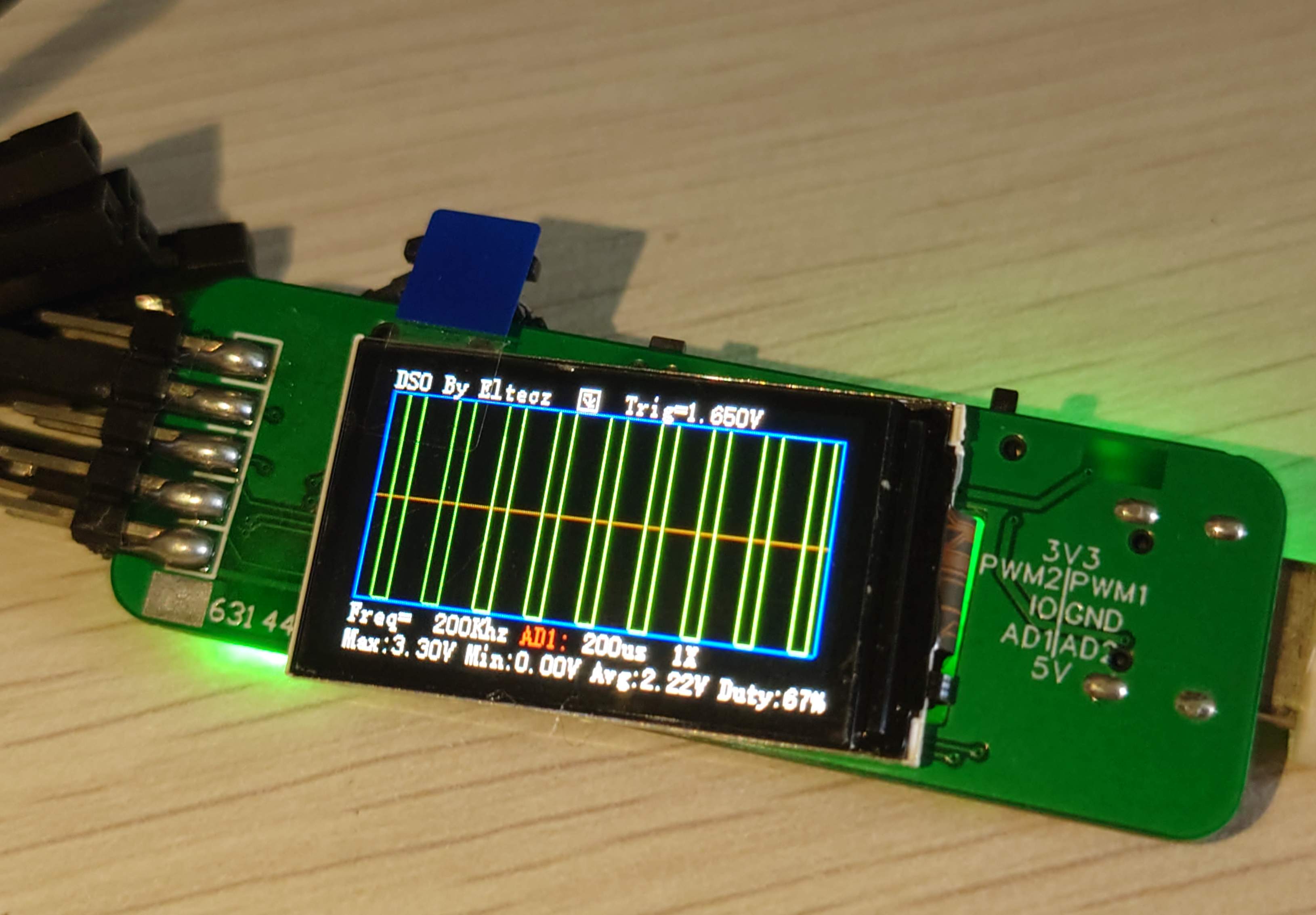
The STM32G030F6P6 microcontroller is used, which supports dual-channel adjustable frequency and adjustable duty cycle PWM output, as well as ADC dual-pass input, and the microcontroller is overclocked to a main frequency of 100M.
The board can also be integrated into other modules for collection.
Display video [link] , open source warehouse [GitHub]
The current functions are:
AD input voltage 0-3.3V
12bits @ 5Mhz/12bits @ 2.5Mhz
1-2-5 time base step from 200ns to 500us
Vertical magnification 1-2-5-10 times
Three triggering methods, 10 trigger levels from 0-90%
Waveform measurement function
1-2-5 time base switching PWM output frequency from 10MHz to 200Hz.
10% step switching PWM output duty cycle from 0% to 100%
3 independent buttons for multi-level menu switching
1 programmable LED light
USB serial port communication is reserved, but I can't get it out.
---------
BOM is not trustworthy, please go to X letter to buy similar packaged components (referring to connectors)
FPC seat must be purchased and connected.
---------
The code is being compiled and is not yet open source. Currently, only firmware downloads are available. It is open source. See above.
If a bug occurs during operation, please send a message via LC Kaiyuan/b site private message/comment area or email. I will modify the program and update it in time.
If you need more cooperation, please only specify the email address Defenver@foxmail.com
------------Explanation session----------
The principle is actually not difficult. Just use DMA+ADC+TIM to cyclically sample, and then transfer the data to the kernel for processing.
According to the actual operation, it is found that the ADC clock can be overclocked. It only needs to ensure that the AXI bus clock is aligned. Therefore, it is overclocked to the ADC clock of 100M, and the sampling delay is appropriately increased, so that the ADC sampling rate reaches the terrifying 5M (TSMC yyds)
The timer uses the TRGO of TIM1 and is connected to the ADC as the clock trigger source. Then the DMA transfers the data to the memory for subsequent processing. You can see the related tutorials of Avnet here to understand the principle.
There is also a PWM output. The principle of this thing is very simple and I won’t explain it. You can refer to Avnet’s tutorial to understand the principle. Generally speaking, compared to other series, G0 has a simpler adjustment method in this aspect.
Next are other peripherals. The previous project used a 0.96-inch screen. Although it was usable, it didn't display much, so I changed it to a 1.14-inch screen here.
The original button felt too bad, so I replaced it with a pulsator switch, and the feel is indeed much better.
The serial port is broken. It seems to be a chip problem. Let's wait for the successor to fix it.
Finally, there is the software part. The software part is not much different from the previous two oscilloscopes. Basically, everything is thrown into while(1) for processing.
The page display part uses the classic point drawing function, the trigger point part uses the ternary operator to judge in order to save code size, and finally the page switching part uses the switch statement with key values to switch options, etc.
The code and ideas of this project are roughly the same.
See the actual picture below
------------

Designed by Eltecz (from OSHWHub)
Design Drawing
 Empty
Empty
Comment