

 Completed
Programmable feedback on switching power supply
PRO Programmable feedback on switching power supply
License
:CC BY-NC-SA 4.0
Description
Project Description
Digital control switching power supply feedback system based on STC8G microcontroller design.
Open Source Agreement
CC-BY-NC-SA-4.0.
Project Related Functions
The output voltage value of the switching power supply is controlled by sending and receiving data through the serial port, and the real-time voltage and current data of the power supply are sent back to the host computer in real time through the serial port. The data can be directly connected to the computer, and the power supply output can be controlled through the computer, or other microcontroller devices can be connected through the serial port. As a host computer.
Project Properties
This project is made public for the first time and is my original project. The project has not won any awards in other competitions.
Design Principles
This program verifies the circuit frame structure of the board. 
The whole is divided into main power supply part.

Digital feedback terminal isolated power supply.

Host computer communication security isolation.

Working Principle:
The output voltage and current value samples the real-time current and voltage through the MCU's built-in ADC channel, and controls the MCU output PWM signal with changing duty cycle through the voltage and current value to feed back to the primary side of the main power supply. (Optocoupler isolation)

The current sampling uses LT199G1, which is modified based on the official original circuit and changed to low-side detection to adapt to current detection of larger voltages. The voltage signal at both ends of the sampling resistor is amplified by LT199G1 and then input to the STC8G-ADC pin. The output of LT199G1 is clamped by a Zener diode to prevent the output voltage signal from being too high and damaging the MCU.


It can also be used as a conventional switching power supply with adjustable output voltage by switching the feedback type.
After switching the jumper cap to regular feedback, the output voltage can be adjusted by the R9 potentiometer on the board.
(Reserved for general feedback-AP4313)

Software Description
The microcontroller program is written based on the STC8G microcontroller (see attachment for program engineering)
Serial port sending and receiving data format.
Note: When downloading the program, the MCU clock frequency is set to 27MHz through the downloader.

The host computer is written using Labview2018.

The communication baud rate needs to be changed to 115200bit before starting.
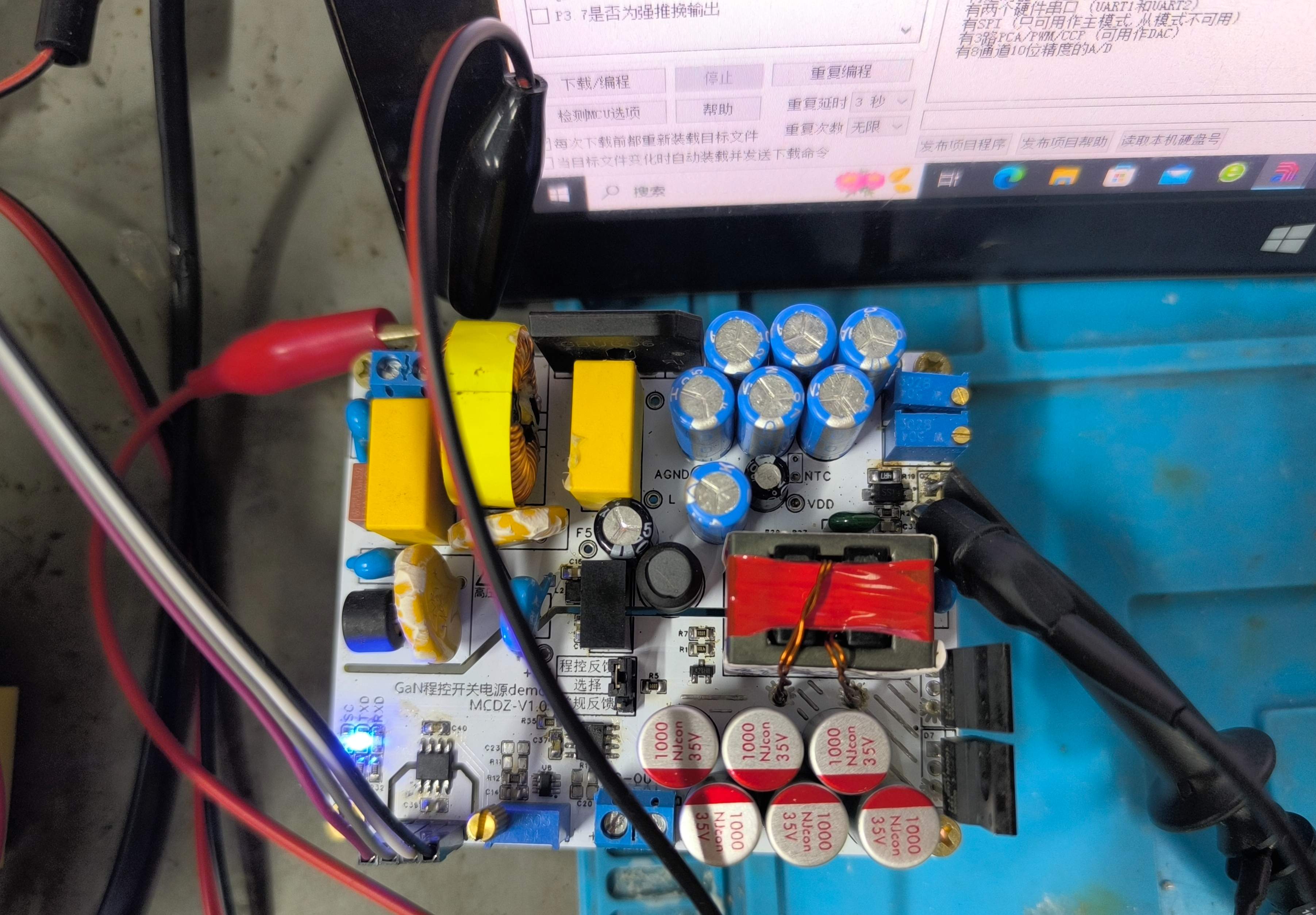
Physical Display
PCB power-on test.


Design Considerations
At present, the key parts of the overall PCB have been tested successfully, but there are still problems with the main power supply part (I hope that someone who is responsible for switching power supply design can help look at the problem. I am just getting started in power supply design, and it is not recommended to use this part of the circuit for the time being) After NCP1342 is powered on, there is a control signal output, but the output frequency is always only 25KHz. The switching frequency of the frequency setting resistor does not change. From the data manual, it is judged that it may be running in low power consumption mode (light load mode), but I don’t know how to exit it. In this model, there is relatively little public information on NCP1342 online. The domestic replacement model PN8213 is not yet available.

If the power tube is welded, it will cause the power tube and NCP1342 to break down. During the overall test, it ran stably once, but after restarting, the power tube and NCP1342 exploded.
Transformer parameters: primary: 0.5mm enameled wire 40T+40T, feedback 0.5mm enameled wire 4T primary 1mm*4 enameled wire 4T (4 parallel) transformer core is ATQ2516.
Other
The attached video is a demonstration test video of the program-controlled feedback part (feedback control boost DC-DC-fb pin) output and collection of real-time voltage and current values, as well as physical power-on status detection and testing.
Designed by 模成Electron (from OSHWHub)
Link:https://oshwhub.com/dingcheng/GaN-Programmable-Switching-Power-Supply-Board
Design Drawing
 Empty
Empty
Comment