

 Completed
Portable Rechargeable Electronic Load
PRO Portable Rechargeable Electronic Load
License
:GPL 3.0
Description
Preface
Before I conceived the idea of making this electronic load (early 2023), I was obsessed with designing a fast charging module, but testing the output current of the fast charging module just required an electronic load to match.
The common solution is to use DC power supply. For my cluttered workbench, it is really unbearable to run another wire for power supply, so I have a self-powered solution.
The design focuses on an all-in-one product that has a simple structure, is suitable for novices, and also looks good.
(Please use the second version, Board2, for PCB proofing)
2023-11-30 Add some instructions for use.

Product Description
Contains lithium battery protection, charging circuit, fast charge trick, and constant current control. Each circuit is almost independent, and can be welded on demand to save costs.
Speaking of cost, a PCB is welded into upper and lower layers, and different components are welded together to form the main body.
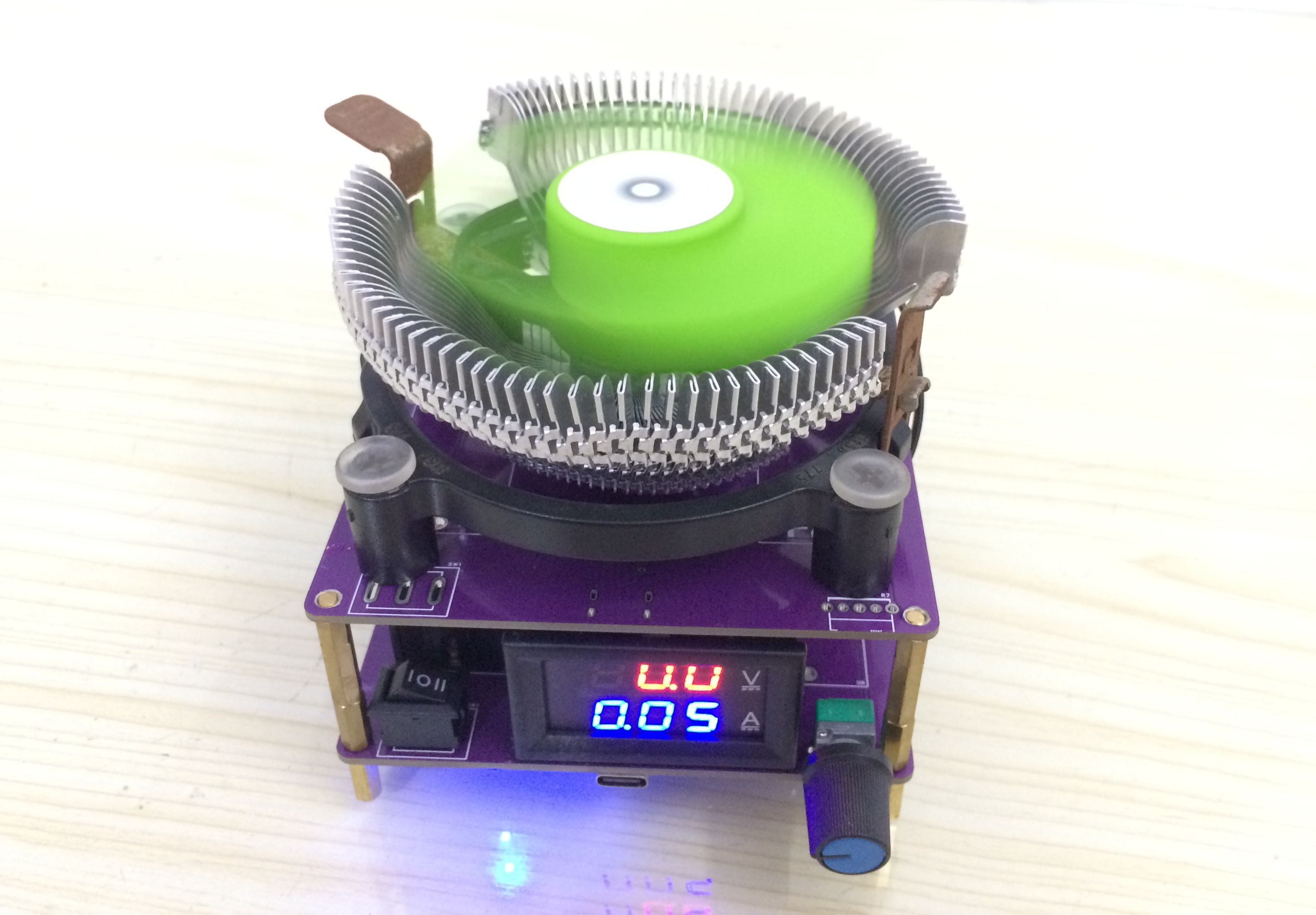
Add a common dual-display digital voltage and current meter, and a CPU fan with free shipping for 9.9 yuan, and the cost can be reduced to the extreme.
Input interface: Type-C, M4 banana socket, supports bare wire access
Design test voltage 0~20V.
Design test current 0~10A.

Circuit Description
1.Lithium battery protection circuit
It uses TP4056 chip, which is a commonly used chip. I won’t explain this too much.
The power control switch is a three-pin three-position switch, which can completely separate the charging and protection circuits. To save costs, you can replace the battery instead of soldering the charging circuit.

2.Lithium battery protection circuit
The commonly used solution is the combination of DW01+8205A, but 8205A is not very welding-friendly, so it is solved by using IP3005A with a larger package, which is directly copied from the manual.

3. Boost power supply circuit
Because most CPU cooling fans are 12V, and the higher the driving voltage, the on-resistance of the MOS tube is relatively smaller, so choose to boost the voltage to 12V.

4.Deception circuit
In fact, to test whether the fast charging module works, this circuit is indispensable. This circuit is a must for me personally.
The circuit contains decoys of different voltages of 5V, 9V, 12V, 15V, and 20V, controlled by a DIP switch.
If you don't need it, you don't need to solder it at all, and it won't affect the test at all.

5.Constant current control
Use LM358 to compare the voltage at both ends of the sampling resistor R8 to control the rapid on and off of the MOS tube to achieve the purpose of constant current control.

First, use TL431 to generate a 2.5V reference voltage. The ratio of R20 and R7 needs to be selected based on the actual resistance of the sampling resistor.
For example, the constantan wire resistance of a dual-display voltage and ammeter is 7.5 milliohms, and the maximum measurement current of the ammeter is 10A.
Therefore, the maximum voltage of the network tag point FB1 is 75mV. In other words, the maximum voltage of the voltage dividing point of R7 is 75mV.
Since R7 is an adjustable potentiometer and is generally not replaced, you only need to change the resistance of R20.
Voltage=2.5V*(10K/R20+10K)
According to the formula, R20 is about 300K, but the voltmeter I use is a little different. I use 51K, so be careful.
In fact, the purpose of the voltage dividing point set here is to limit the maximum constant current and prevent collective smoke from being caused by excessive discharge current!
Top Priority: welding assembly
Four partial circuits are welded on the bottom of the lower PCB, including lithium battery protection, charging, voltage boosting, and constant current control.
Weld the switch, battery holder, and potentiometer on the top surface of the lower PCB.
The three-pin three-position switch is not connected yet to facilitate power-on testing of each part. In fact, as long as the welding is correct, there will be no smoke~~~

Then there are the welding components on the top surface of the lower layer and the top surface of the upper layer, including the wiring of the digital voltage and ammeter.
The upper MOS tube is flip-chip, and the heat sink is facing upward for contact with the heat sink. Just align the holes of the heat sink with the holes on the PCB.
The competition LOGO is also displayed here.

The upper and lower wires are connected, the power supply interface of the general voltage and ammeter, and the CPU fan power interface are all welded on the lower layer.

The perspective after unfolding the two PCBs.

The upper and lower PCBs are connected through copper pillars.
M3x12+6, two sections; M3x18+6, one section.
If the funds are average, use ordinary nuts to fix the top. If the funds can be reimbursed, use patch nuts, which is beautiful and neat.

The four holes on the outer side of the upper layer are used to fasten the CPU fan. The old 775-pin fan or the popular dual-purpose fan can be installed in place.

Basic Usage
Three-legged three-position switch, the three positions from left to right correspond to [Charging], [Neutral] and [Power Supply].
[Neutral] completely cuts off the connection between the lithium battery and other circuits to avoid unnecessary loss of power.
When you turn it to the left, the lithium battery is connected to the charging circuit and can be charged.
When turned to the right, the lithium battery is connected to the boost circuit, which is equivalent to an ordinary power switch and enters the working state.
The potentiometer is used to adjust the constant current. The maximum discharge current is set by changing the R20 resistor as mentioned above.


The fast charging decoy chip CH224K has a voltage resistance of about 24V. When not using the decoy, try to disconnect the power supply of the chip and only turn the first bit of the DIP switch to ON when needed.


There is a detail that needs to be paid attention to during the final production, that is, before welding the potentiometer, you must measure whether the minimum value can be returned to zero.
This resistance will directly affect the minimum constant current control after power-on. The good quality is 0.07A, and it is almost 0.7A. If the requirements are not high, it can be ignored.
One of the video demonstrations below uses a poor quality potentiometer.

One Hundred Thousand Whys Quick Questions and Answers
1. How long is the usage time?
> Generally, one battery is enough for a short test time. Two battery boxes can be installed to increase the use time.
2. Can it test voltages above 20V?
> Just replace the MOS tube with a higher voltage resistance.
3. Can the test current exceed 10A?
Ammeters with a current greater than 10A need to use a shunt, which takes up a lot of space and is difficult to insert into it.
Solution: You can use several sampling resistors in parallel and attach them to the PCB. You need to calculate the same resistance value to enhance the PCB’s conductivity.
In general, it is possible but not recommended.
4. Do all circuit components need to be welded?
> In addition to the constant current control part, other parts can be selectively welded, that is, you can weld the corresponding components according to the parts you need to use.
5. Think of continuing to add more.
Designed by hungryheart66 (from OSHWHub)
Design Drawing
Intellectual Property Statement & Reproduction Instructions
This is an open-source hardware project. All intellectual property rights belong to the creator. The project is shared on the platform for learning, communication, and research only; any commercial use is prohibited. If your intellectual property rights are infringed on EasyEDA, please notify us by submitting relevant materials in accordance with the Rules for Complaints and Appeals of IPR Infringement.
Users must independently verify the circuit design and suitability when replicating this project. All risks and consequences are borne by the user, and the platform assumes no liability.
 Empty
Empty
Comment