Editor Version ×
recommended

Pro Edition

free

Brand new interactions and interfaces

Smooth support for design sizes of over 3W

devices or 10W pads

More rigorous design constraints, more

standardized processes

For enterprises, more professional users

Std Edition

Easy to use and quick to get started

The process supports design scales of 300

devices or 1000 pads

Supports simple circuit simulation

For students, teachers, creators

Completed

PRO MakerLab PCIe to M.2(NVMe protocol) adapter card

PCIe to M.2(NVMe protocol) adapter card

Project tags

License

GPL 3.0

License: GPL 3.0

Mode:

Mode

Editors' pick

Editors' pick

  • 103
  • 0
  • 0
Update time: 2024-12-02 02:38:49
Creation time: 2024-12-02 02:05:03
Description

Description

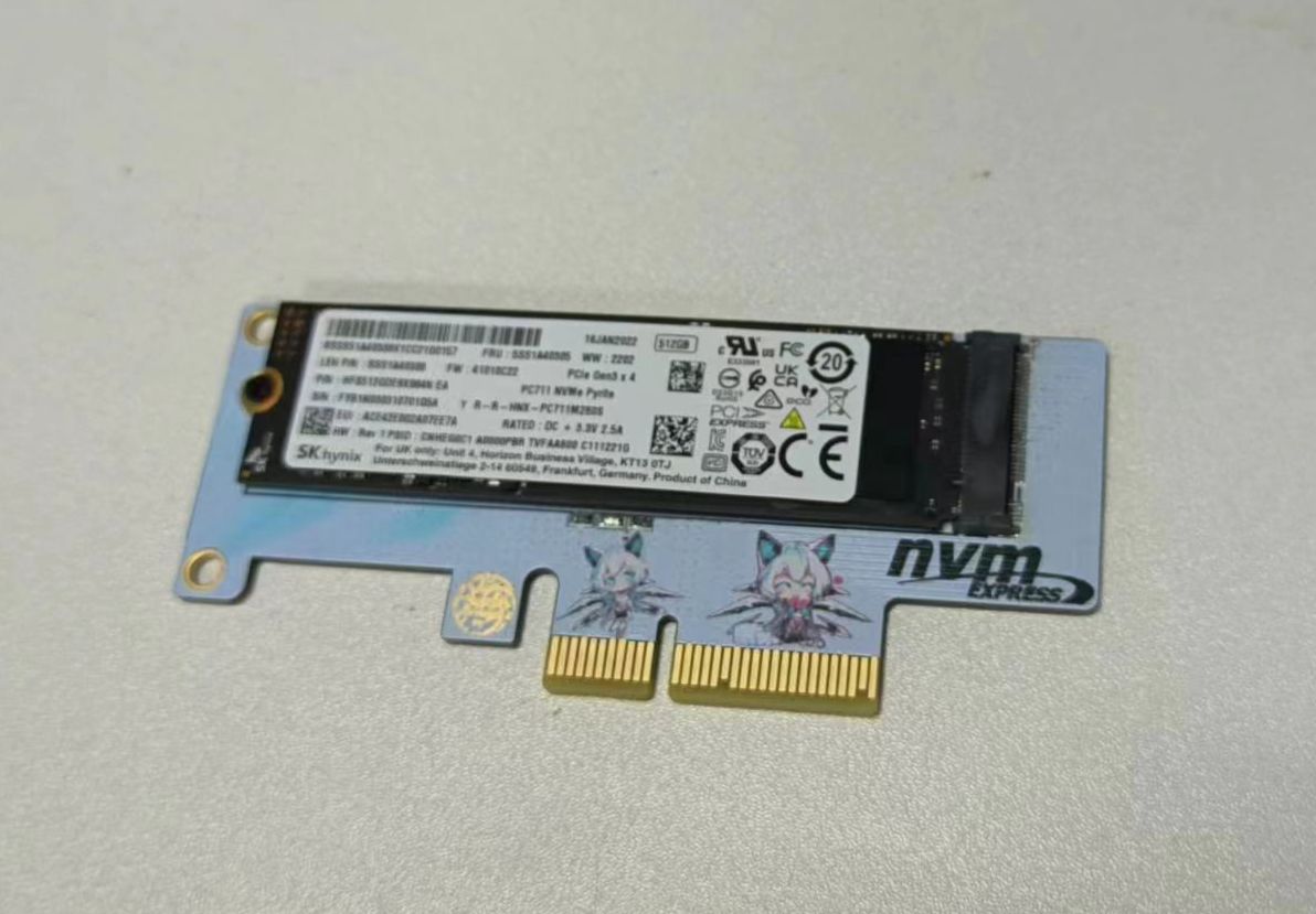
# 1. Introduction What is PCI-E? In short, PCI-E is a computer interconnect bus standard proposed by Intel in 2001 to replace the previous PCI and AGP. It is characterized by serial (the previous ISA, PCI, AGP, etc. are all parallel), and supports 1 to 32 lanes (although the most common and longest is the most commonly used X16 on graphics cards), and the speed is shown in the table below. ![20210413030040274.jpeg](//image.lceda.cn/pullimage/NgfCEKvz6FHmcrtiOug9011WmsWkTQUpzHSogQq4.jpeg) Since the signal transmitted by PCI-E is a differential signal, it is necessary to explain the definition of differential line here: Comparison between phase signal and single-ended signal: the traditional single-ended signal is transmitted by the potential difference relative to the ground wire, so only one ground wire is needed, and only the corresponding number of signal lines are required to transmit several signals; The differential signal uses a common ground wire (potential is 0), when transmitting a signal, two signal lines are needed, one is positive relative to the voltage of the ground wire (the electric potential is positive), the other voltage is negative (the electric potential is negative), the absolute value is the same (phase difference of 180 degrees), the potential difference between the two signal lines is used to transmit the signal, but two signals are transmitted, if one signal line is 3.3V, the other signal line is -3.3V, and the ground wire is 0. This seemingly wasteful transmission method actually has many advantages: first, because the ground wire can be controlled, it will not cause the difference of the ground wire due to the voltage drop caused by the wire length, and then the transmission voltage can be reduced to reduce power consumption (the early AGP 2X works at a voltage of up to 5V, Second, because the influence of electromagnetic interference on the two signal lines of the differential signal is almost the same, even if there is interference, the high potential is still higher than the low potential, while the single-ended signal may turn the low potential into a high potential due to interference, resulting in transmission errors, so the differential signal is highly anti-interference. Today, most high-speed serial interfaces use differential signals, such as USB3.0/3.1, PCI-E, HDMI, Ethernet, etc. # 2. Interface definition ## 1.PCI-E ### Slot There are 4 interface sizes, each with the same pair of pins from 1 to 11, and the rest is that the number of differential and clock data lines is different, and the corresponding PCIe size is different. ![Quicker_20231002_100809.png](//image.lceda.cn/pullimage/pOqoPsPMRbpvlfDjld4km6J9Vq8moqGcgr2deRCZ.png) ### Pin function definition ![20210717222654391.png](//image.lceda.cn/pullimage/PTXsHPNSzJlOqEqsy7THbXQVt7NXg1FeiTt1ngd6.png) ## 2.M.2 interface The M.2 interface has two buses, SATA and PCIE, and the protocols are AHCI/NVME, which is a non-volatile memory express interface. ![Quicker_20231012_203549.png](//image.lceda.cn/pullimage/fVNMknNBgENbFmvYFRFhMt1xLmE0hdj6kyBHBaCr.png) ### Mechanical structure The M.2 connector uses the notched position of the PIN to indicate the key, a concept used to indicate the interface/protocol supported by the module. In the current specification, there are five key bits defined in the current specification: A, B, E, F, and M, among which B and M are the most common. ### Typical Applications A-Key: Mainly used in wireless connection, such as WiFi, Bluetooth, NFC, Wigig. The types of cards include 1630, 2230 and 3030. B-Key: Mainly used in WWAN, GNSS, SSD. The types of cards include 3042, 2230, 2242, 2260, 2280 and 22110. E-Key: Mainly used in wireless connections, such as WiFi, Bluetooth, NFC, GNSS. The types of cards include 1630, 2230 and 3030. M-Key: Mainly used in host interfaces that support PCIe or SATA protocols, usually SSDs. Special: There are three types of M.2 connectors (Socket 1, 2, 3), because Socket1 is all soldered and only applicable to 1216, 2226 and 3026 sizes, so the common M.2 device connectors are mostly Socket2 and Socket3. B-Key's module, with its PIN notch in slot 1219, provides support for PCIe x2, SATA, USB 3.0, I2C, HSIC, and more. M-Key's modules, with their PIN notch at slot 5966, provide support for PCIe x4, SATA, and SMBus. M.2 SSDs are almost always "B & M" Key, which means that there are two notches. Among them, the configuration that supports SATA or PCIe x2 is called the "Socket 2" configuration, and the configuration that supports PCIe x4 is called the "Socket 3" configuration. ### Pin function definition M.2 PCIE SSDs are M-Keys ![20170223172404189.jpg](//image.lceda.cn/pullimage/yTbdWC40dDgyMvz8pYWF2OHdwZtyZGWYjDWTacH5.jpeg) ![20170223172409460.jpg](//image.lceda.cn/pullimage/RpmuPMvu04kDBy1I3XIlIgdet9IuoeNY8pYPRkNR.jpeg) SATA SSDs include B-Key & M-Key ![20170224092721544.jpg](//image.lceda.cn/pullimage/WUDj7b7VglMNEmTkz3gcuiTJ6ufrhy203DwNr1tY.jpeg) ![20170224092726942.jpg](//image.lceda.cn/pullimage/Vxqbm9ChtZpbKTFOnYLn91gvLkmIlCpueJDJSB19.jpeg) # 3. the main points of the design ## 1. Impedance control The differential impedance given in the PCIe specification is 100Ω and the single-ended impedance is 50Ω. But you must have seen the following description: PCI Express link traces must maintain 100Ω differential /60Ω single-ended impedance for 4-layer or 6-layer boards; and 85Ω differential/ 55Ω single-ended impedance for 8-layer or 10-layer boards. The specific explanations are as follows: Because the higher the number of layers on the board, the closer the traces are to the reference plane, the smaller the impedance will be, so the target impedance value of the design should be reduced in order to match the impedance. At the same time, the density of the multilayer board will also increase, the line width will decrease, the smaller the line width, the greater the impedance, and the transmission loss will increase, so the more layers, the shorter the trace length will be required (in order to control the transmission loss). ## 2. Precautions for gold finger and connector 1. The edge finger pads of the reference plane should be removed to meet the impedance target. 2. The edge part of the finger along the entire length should be removed. 3. The two traces of the differential pair line should become a domain of connector pins from the same layer. 4. In order to satisfy the impedance target, the reference plane below the edge finger should be removed. 5. And the entire reference side under the gold finger must be completely deleted. The 2 signals of the differential pair should be routed on the same layer to connect to the pins of the connector. ## 3. Other precautions 1. The differential pair meets the 3W spacing in the inverting phase and the 5W spacing in the same phase. 2. The length of the positive and negative lines of the PCI-E difference line must meet the matching requirements, but the length between the difference lines does not need to match. 3. Polarity ensures the opposite. 4. PCI-E does not support LANE rollover. 5. PCI-E chips, especially the reverse side of the PCB of the PCIE signal line, should try to avoid high-frequency signal lines, and it is best to pour copper on the ground in full GND. 6. When designing the PCB, a high-frequency decoupling capacitor of about 0.1uF should be placed near each pair of power pins of the PCIE chip, not too far away from the chip. 7. The power supply connected to the PCIE chip or the vias on the GND cable use a large via, double via, or dual loop power supply. 8. The gold finger of the PESET# pin signal of PCIE is designed with a gold finger of about the same length as PRSNT1#. 9. The gold finger part is not allowed to be covered with copper, and each layer should be mined with copper. # 4. physical testing Take a notebook and disassemble the disk to make do (now use it as a portable hard disk) SK Hynix BC711 (OEM version) 512G (almost full) ![微信图片_20231012213757.jpg](//image.lceda.cn/pullimage/ygqB8wYoiAJ1IMzWiOWi1gA92HFOtmPEpv71Cf72.jpeg) ![Quicker_20231012_133813.png](//image.lceda.cn/pullimage/uHKZ3Q1ohUZbeIz5QPKTfEAzg942bKW00YNavw1K.png) The write is a bit inferior, but eighty percent is due to the full disk, and there is not much difference compared to the motherboard's built-in interface. Try again next time there is an empty disk of idle PCIe4.0 (too lazy to disassemble) # 5. Miscellaneous ## 1. PCI-E stackup and reference plane Typical PC motherboards are designed with 4 layers of stacks, while server, workstation, and mobile system motherboards use 6 or more layers of stacks. The card can be stacked with 4 layers or 6 layers. Use 0.5OZ copper-plated microstrip wire and 1OZ copper strip wire. The overall board thickness of the card must be 0.062inch. The PCB thickness of the mobile platform can be 0.062 inch or 0.050 inch. In order to minimize loss and jitter budgets, the most important consideration is the target impedance of the design, and the tolerance of the impedance should be kept small enough. A thicker dielectric layer and wider traces will reduce losses. Microstrip differential lines produce greater impedance changes than strip differential lines. The signal corresponds to avoid discontinuities in the reference plane, such as segmentation and voids. When the signal line changes layers, the vias of the ground signal should be placed close to the signal vias. The recommendation for each pair of signals is to put at least 1 to 3 ground signal vias. Also, never let a line go across a plane split. ## 2. About AC coupling capacitors The measured speed has little impact (maybe I didn't try 4.0?) And PCIe and M.2 are directly connected, and if there is no chip, it will be deleted simply. If you want to know more, you can go down to the original article 6 (M.2 interface circuit design) I won't repeat it here. ## 3. About the M.2 interface You must buy an M-Key, otherwise you will not be able to connect to an M.2 hard drive. In addition, M-Key can replace B-Key to a certain extent, and it has a wider applicability. For example, M.2 hard drives with SATA protocol do not have to use B-Key. In addition, the M.2 interface can be difficult to solder, and the solder wire should help a little. Before powering on, remember to check whether the M.2 interface has virtual soldering, tinning, etc. # Compiled from ------ 1. [PCIE bus hardware design](https://blog.csdn.net/sinat_15677011/article/details/116923732) 2. [PCIE-PCB Design Specifications! (Recommended collection)](https://blog.csdn.net/ybhuangfugui/article/details/110507863) 3. [PCI-E High-Speed PCB Place-and-Lay Design Guide](https://blog.csdn.net/qq_37457748/article/details/96788955) 4. [A brief explanation of the pin definition of PCI-E (memo)](https://blog.csdn.net/u011488769/article/details/115652089) 5. [PCIx Series "PCIe Bus Hardware Design"](https://xilinx.eetrend.com/blog/2018/100016695.html#:~:text=PCIe%E8%A7%84%E8%8C%83%E4%B8%AD%E7%BB%99,%E7%AB%AF%E9%98%BB%E6%8A%97%E4%B8%BA50%CE%A9%E3%80%82) 6. [M.2 interface circuit design](https://blog.csdn.net/weixin_42107954/article/details/126271633) 7. [Definition of SSD interfaces based on the SATA3 protocol and PCIE protocol based on the M.2 interface](https://blog.csdn.net/u011400634/article/details/103117878)
Design Drawing

Design Drawing

schematic diagram
1 /
PCB
1 /
The preview image was not generated, please save it again in the editor.
Empty
Project Attachments

Project Attachments

Empty
Project Members

Project Members

Target complaint
Related Projects
Change a batch
Loading...

Comment

Add to album ×

Loading...

reminder ×

Do you need to add this project to the album?

服务时间

周一至周五 9:00~18:00
  • 0755 - 2382 4495
  • 153 6159 2675

服务时间

周一至周五 9:00~18:00
  • 立创EDA微信号

    easyeda

  • QQ交流群

    664186054

  • 立创EDA公众号

    lceda-cn