

 Completed
[Network first ] ZYNQ7035 core board and high-speed ADC
PRO [Network first ] ZYNQ7035 core board and high-speed ADC
License
:CC BY 3.0
Description
Project Description
This project is expected to open source ZYNQ7035 core board and an 8-bit 1GSPS 4-channel ADC module. The 7020 core board and RF module of the previous project are biased towards general-purpose and electric competitions; The 7035 core board and high-speed ADC are biased towards high-speed communication, high-speed electronic measurements such as 1GSPS 4-channel oscilloscopes. The ZYNQ7035PS end is a dual-core cortex-A9, and the PL side is based on the kintex 7 architecture, which is better than the Artix7 architecture of the 7020 and 7010, and has stronger timing control capabilities.
The PL side of the Logic Cells is 275k, which is more than 3 times that of the 7020 and nearly 10 times that of the 7010. Among them, the DSP resource is more than 4 times that of the 7020, which makes the filter design steeper and can deploy a larger scale of DSP algorithms. At the same time, the BRAM resource is more than three times larger than that of the 7020, and the ILA can capture more data for easy commissioning.
Compared with the ZYNQ7035 of 3000-4000 yuan on TB, the BOM cost of this open source core board is only a few hundred yuan, which provides a strong help for all electronic enthusiasts who need ZYNQ7035, and this project is the first open source 7035 of the oshwhub platform, and! It seems to be the first on the whole network!


Of course, not only the ZYNQ7035 core board, but also the HMCAD1511 8bit 4-channel 1G sampling rate high-speed ADC module and driver will be open-sourced.

Open-source protocol
Commercial use is prohibited without the permission of the author. Reprinting or citation should indicate the original author and the link to the project
Project-related features
Resource Introduction:
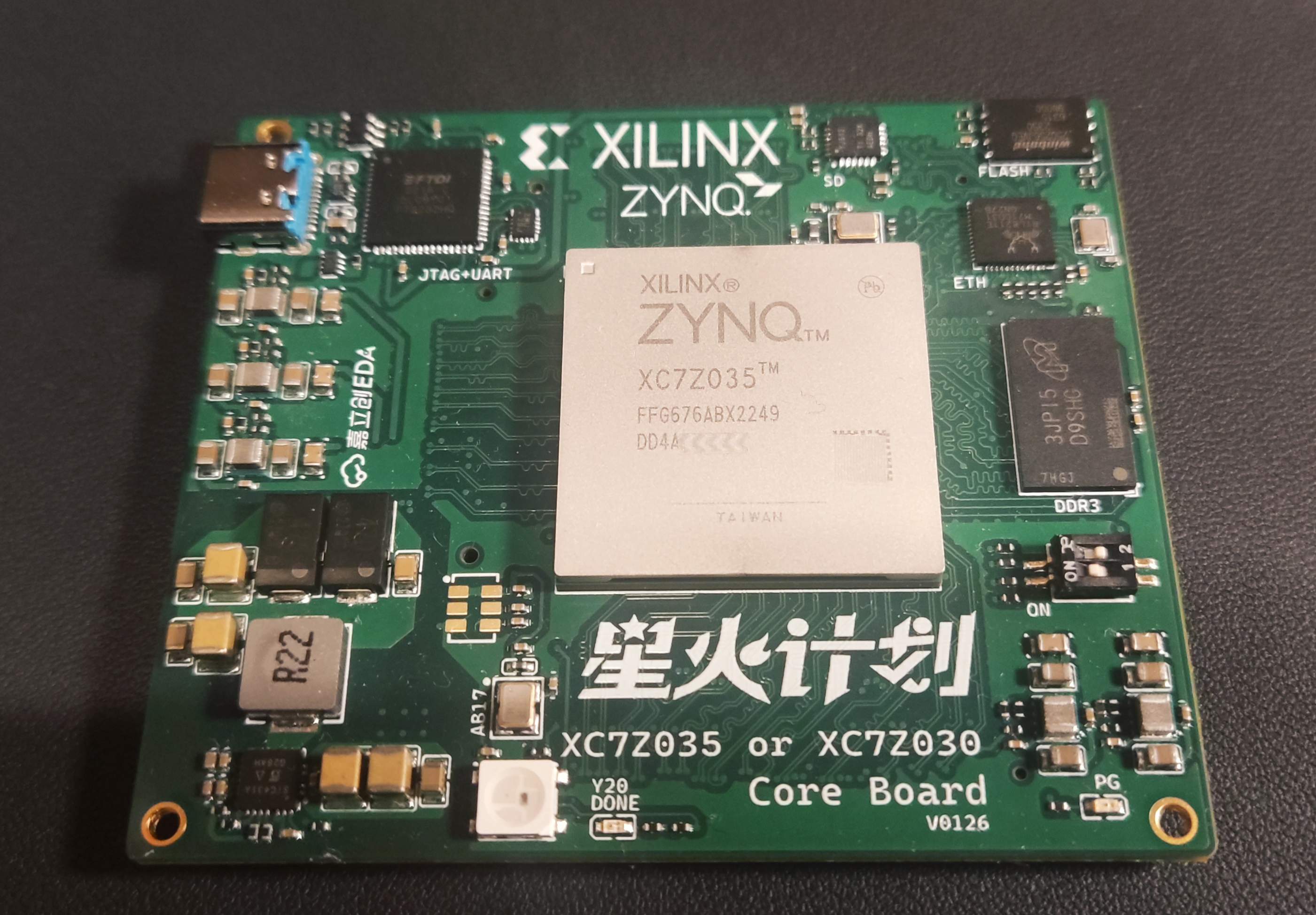
(1) ZYNQ7035 core board PS side: 1 DDR3, QSPI FLASH, SD card adapter chip, Gigabit Ethernet, JTAG, UART on board.
(2) TYPEC port explanation (emphasis added!!) ): Use FT2232 chip, complete the operation of a single chip JTAG+UART, the USB port uses TYPEC, contains ESD+ common mode filtering and an ideal diode anti-current backfill, no longer need to debug, power supply, burn a lot of wires (there are even a variety of ancient USB interfaces. ONE WITH TYPEC IS ENOUGH! Gospel for developers~
(3) Power management: Vishay SIC431 is used for core power supply, with remote sampling, high efficiency (97 % peak efficiency), and 24 A power supply capability. The device is internally compensated and does not require an external ESR network for loop stability. The auxiliary power supply is TPS82130, our old friend:) The power-on sequence is shown in the figure

(4) ZYNQ7035 PL end :P L end of the core board lead to a set of GTX BANK; 36 pairs of differential equal length High Performance BANK with a level of 1.8v, 35 pairs of differential equal length High Range BANK with a level of 3.3v, a total of 158 ios, limited by the 6-layer board did not lead to more IO, but it was enough to use.
(5) ZYNQ7035 baseboard: This time a matching baseboard is open-sourced, in which HRbank is led out as a PMOD interface (PMOD is a good civilization!) ), HPbank leads out for the BTB connector. The PS side gives an Ethernet interface, two 2510 power supply ports, an SD card interface, an LDO to power the PMOD, and a power protection IC with fast overvoltage clamping, adjustable overvoltage lockout, adjustable current limit, adjustable output slew rate control, and overtemperature protection. Since there is no equipment to test the GTX for the time being, the base plate does not lead to the GTX, and you can draw it yourself if necessary.
(6) HMCAD1511: 8bit 1GSPS ADC, analog front-end is LMH6521 high-performance dual-channel DVGA, -3dB bandwidth is 1.2Ghz. The input impedance is 50Ω, the programmable gain, the dynamic range is 31.5dB, and the step size is 0.5dB. On-board phase-locked loop HMC832 with sample clock. The interface uses 1.8V LVDS. On-board power management, using an integrated DCDC and ultra-low noise ultra-high PSRRLDO, with through-center capacitor filtering, and an input of 5V 2510 interface.
Project properties
This project is the first public and is my original project. The project has not won an award in another competition.
Project progress
(a) ZYNQ7035 Core Board:
(1) ZYNQ chip: normal work, VIVADO normal connection:

(2) DDR3: Normal Working, 0 Errors:

(3) JTAG+UART: FT2232 works normally, and both JTAG and UART can be used normally.
(4) Ethernet: RTL8211 works normally, network loopback test results:

(5) Curing and start-up: QSPI FLASH curing results, offline start-up results:


(b) HMCAD1511:
The work is normal, Figure 1 shows the data test mode, you can see that all channels are working normally. Figure 2 shows the ILA acquisition data imported into MATLAB for processing, and the FFT and time-domain waveforms are shown in the figure.


Design Description
1. ZYNQ7035 core board:
(1) Power supply: Vishay SIC431 is used for core power supply, with a maximum output of 24A current. The auxiliary power supply uses a DCDC converter TPS82130 an integrated inductor, which can output a maximum of 3A and a total of 6 voltages. The power-on sequence is 1V0->1V8->1V2&2V0->1V5&3V3. For detailed specifications and requirements, please refer to the official Xilinx manual.


The core power supply test result is 999.5mV error 0.5 thousandths. The ripple is 8mV per peak and 500uV RMS, which meets the official requirements of Xilinx.


(2) DDR3 :D DR3 uses Micron's monolithic MT41K256M16 monolithic 4Gbit.

(3)FLASH:QSPI FLASH采用W25Q256JVEIQ(或W25Q128JVEIQ)

(4) SD card adapter: The SD card adapter uses TI's TXS02612RTWR
(5) Ethernet: Ethernet adopts REALTEK's RTL8211

(6) Clock: PS adopts 33.3333MHZ 20ppm active crystal oscillator, PL adopts 100Mhz 20ppm active crystal oscillator. GTX USES 125MHZ DIFFERENTIAL CRYSTAL OSCILLATOR (LVDS)
(7) JTAG+UART: using FT2232HQ, a single chip to complete two tasks.
(8) BOARD-TO-BOARD CONNECTOR IO RESOURCES: PL TERMINAL LEADS TO A SET OF GTX BANKS; 36 pairs of differential equal length High Performance BANKS at 1.8 V and 35 pairs of differential equal length High Range BANKS at 3.3 V with a total of 158 ios. PS leads to ETH, SD card, JTAG, and the rest of the pins can be implemented by EMIO using PL pin resources if necessary.
(9) Boot mode selection: There are three boot modes, namely JTAG boot, QSPI FLASH boot, and SD card boot. Changes can be made via the DIP switch on the core board:
| Startup mode | Switch 1 | Switch 2 |
| JTAG starts | ON | ON |
| QSPI FLASH BOOTS | ON | OFF |
| SD card boots | OFF | OFF |
(10) ZYNQ chip model: XC7Z035-FFG676, XC7Z035-2FFG676, XC7Z030-2FFG676, XC7Z030-FFG676
Software Description
(1) The ZYNQ7035 section gives UART, RGBLED, DRAM, and Ethernet test projects, see the attachment, and the VIVADO version is version 2022.1
(2) The driver engineering of the HMCAD1511 is zynq Ultrasale + MPSOC XCZU3EG (interface definition compatible ZYNQ7035 backplane, if you need to migrate it yourself), see the attachment, and the VIVADO version is version 2022.1
Physical display


Design considerations
(1) When soldering the Zynq core board, it is recommended to solder the power supply now, test the normal power supply voltage, and then solder the penetrating capacitor and other chips after the starting sequence is normal, so as to prevent the chip from being damaged due to abnormal power supply.
(2) It is recommended to use BGA soldering station for welding steel cover ZYNQ7035 chips, not single air gun welding, or choose JLC SMT to paste directly.
(3) Suggestions for soldering sequence: power supply - BGA chip - front peripheral circuit - reverse capacitor resistance - each connector.
(4) After the welding is completed, it can be verified by the RGBLE test program in the programming accessories.
(5) FT2232HQ program burning: Note that FT2232 to JTAG+UART requires program support, and cannot be used without burning. For vivado 2022 version, it comes with support for FT2232, and the program can be burned by following the steps below:
(1) Open Vivado (any project) and connect the core board typec (plug in the line).
(2) Open Device Manager to check if there is a new USB device plugged in, if not, there is something wrong with the hardware. Under normal circumstances, as shown in the figure, there is a USB Serial A and B connection

(3) Open the TCL of vivado, enter program_ftdi -write -ftdi FT2232H -serial 0ABC01 -vendor "my vendor co" -board "my board" -desc "my product desc" Enter and send, wait for a while to display INFO: FTDI Programming Passed After the program is burned, configure the FT2232 A port as JTAG and B port as UART. Then you can use the ZYNQ7035 happily~


(6) For the protection of the USB port, the ideal diode withstand current for anti-backfill is selected at the 2.5A position, and the power of the whole version is limited to 12.5W. Generally speaking, 10W is completely sufficient for ZYNQ7035.
(7) The core board of the ZYNQ7035 is Jialichuang 6-layer plate plate in the hole process, 3133 laminated, and the impedance can be selected free of ± 20%. HMCAD1511 is a 4-layer board 7628 stack.
Description of project attachments:
(1) Due to the upload 50M limit, the test program will be sent to Baidu network disk: ZYNQ7035 test program Extraction code: SDMY
(2) The detailed demonstration and explanation video will be posted on station B, the link is at the top of the comment area, and the project attachment is ZYNQ7035 start the video from FLASH.
Designed by 上电冒烟 (from OSHWHub)
Link:https://oshwhub.com/z_star/zynq7035-core-board-and-high-speed-adc
Design Drawing
Intellectual Property Statement & Reproduction Instructions
This is an open-source hardware project. All intellectual property rights belong to the creator. The project is shared on the platform for learning, communication, and research only; any commercial use is prohibited. If your intellectual property rights are infringed on EasyEDA, please notify us by submitting relevant materials in accordance with the Rules for Complaints and Appeals of IPR Infringement.
Users must independently verify the circuit design and suitability when replicating this project. All risks and consequences are borne by the user, and the platform assumes no liability.
 Empty
Empty
Comment