

 Completed
[ MCU ] Simple LCD1602 temperature electronic clock
PRO [ MCU ] Simple LCD1602 temperature electronic clock
License
:GPL 3.0
Description
1 Project Introduction
Based on the simple LCD1602 temperature electronic clock designed by the STC89C89C52RC-40I-PDIP40 single-chip microcomputer, the overall PCB size is as large as the size of the LCD1602 LCD screen (80×37mm), with the function of real-time display of time and temperature, 3 buttons control the time setting/plus/subtraction respectively, and the buzzer will have a prompt sound when the button is pressed.
2 General design
Simple LCD1602 temperature electronic clock, the main control single-chip microcomputer uses STC89C89C52RC-40I-PDIP40, the power input is 5V, the Type-C interface of 6P direct insertion is adopted, the button uses a 6×6×6mm horizontal package, the buzzer sounds when the button is pressed, and the DS1302 real-time clock chip detects the current temperature DS18B20 the temperature sensorLCD1602 LCD screen displays real-time time and temperature.

Fig.2-1 Block diagram of a simple LCD1602 temperature electronic clock system
3 Hardware Design
3.1 Power Circuits
The power supply uses a 6P in-line Type-C interface, and C1 is the power filter capacitor.
 Fig.3-1 Type-C power input入
3.2 The minimum system circuit of the single-chip microcomputer
The main control is STC89C89C52RC-40I-PDIP40 single-chip microcomputer, plug-in package, easy to solder, P0 port is special, there is no pull-up resistance inside, so the I/O port must be connected to an external pull-up resistor of 4.7K~10K. When P0 is used as an address/data multiplexing bus, it is a low 8-bit address line [A0~A7] and a data line [D0~D7], so there is no need for an external pull-up resistor. About EA# (EA# pin has been pulled up to VCC internally), if the external pull is not added or the external pull is pulled up to VCC, the MCU will start to execute the program from the inside after power-on reset; If the external pulls down to the ground, the microcontroller starts to execute the program from the outside after the power-on reset.
The external RST pin is reset, the capacitance is 10uF, the resistance is 10kΩ, through the RST1 button, the RST reset pin is pulled high, release the RST1 button, the RST reset pin is pulled low, and an external reset pulse is generated to reset the system. This signal source that pulls up the reset pin to generate a reset needs to be held for 24 clocks plus 10us to produce a reset, and then the RST pin is pulled low to end the reset, and the microcontroller starts to work normally from 0000H of the user program.
The function of the crystal oscillator is to provide the clock signal to the minimum system of the single-chip microcomputer, the crystal oscillator frequency X1 is selected as 11.0592MHz, and the resonant capacitance is 47pF, which is used to ensure that the output oscillation frequency is more stable.
 Fig.3-2 Minimum system circuit of STC89C52RC MCU
3.3 LCD1602 LCD screen
LCD1602 the LCD screen has low power consumption, it is directly connected to the P0 port of the main control single-chip microcomputer and P2.5, P2.6 and P2.7, and the power supply directly uses the VCC (+5V) of Type-C input, V0 is the contrast adjustment end of the LCD1602 LCD screen, and the display contrast can be changed by adjusting the resistance of the RP1 adjustable resistor, and a ghost will be produced when the contrast is too high.
 Fig.3-3 LCD1602 LCD display module
3.4 DS1302 Real-Time Clock
The DS1302 real-time clock chip counts seconds, minutes, hours, days, weeks, months, and years with leap year compensation, using synchronous serial communication using only three wires: RST (reset), I/O (data line), and SCLK (serial clock). The DS1302 operates at very low power consumption, consuming less than 1μW of power to hold data and clock information.
 Fig.3-4 Pins of the DS1302
 Fig.3-5 Internal block diagram of DS1302
VCC2 (prime power supply) is directly connected to the Type-C input VCC (+5V), and VCC1 (backup power supply) is connected to a 3V CR1220 coin cell battery for backup, so that time information and data can be stored in the absence of main power supply. When VCC2 is greater than VCC1+0.2V, the DS1302 is powered by the VCC2 mains supply. When VCC2 is less than VCC1+0.2V, the DS1302 is powered from a VCC1 backup supply. The DS1302's crystal oscillator is directly connected to 32.768kHz. SCLK (Serial Clock Input), I/O (Data Input/Output) and RST (Reset) are directly connected to the P1.1, P1.2 and P1.3 of the microcontroller.
 Fig.3-6 DS1302 real-time clock module
3.5 DS18B20 temperature sensor
DS18B20 temperature sensor can provide temperature measurement with 9 to 12 bit resolution, using a single bus protocol, through a single wire port (DQ) to communicate with the P3.7 port of the microcontroller, which needs to be connected to a weak pull-up resistor.
 Fig.3-7 Internal block diagram of DS18B20
 Fig.3-8 DS18B20 temperature sensor module
3.6 Buzzer circuit
The P1.0 port of the single-chip microcomputer is used for control, due to the limited driving current of the single-chip microcomputer, a digital trilode can be added to drive to improve the output capacity. Here, the NPN type 8050 triode is selected to drive, and when the transistor works in the switching state, the driving current is amplified to make the buzzer sound.
 Fig.3-9 Buzzer circuit
3.7 Key circuit
The key control part is mainly composed of 3 independent buttons, directly connected to the P2.2, P2.3 and P2.4 ports of the single-chip microcomputer, and the other side and the key fixed support pin are connected to GND, you can enable the internal IO pin pull-up mode of the single-chip microcomputer, the default pin is high, if the key is pressed, the pin will be connected with GND, at this time it is low, check whether the key is pressed by checking whether the IO pin of the corresponding single-chip microcomputer is low. In order to avoid the false triggering of the key, it can be debited in the software.
 Fig.3-10 Key circuit
3.8 Download Interface
The program is downloaded using the UART communication protocol serial port for burning, with 4 Pins, with TTL levels, the low level is 0 (0V), and the high level is 1 (5V). The serial port on the single-chip microcomputer is generally two ports, one is the TXD transmitter and the other is the RXD receiver. When connecting the USB to TTL cable, pay attention to the cross interconnection, that is, the RXD of the USB to TTL cable is terminated to the TXD end of the single-chip microcomputer, and the TXD is terminated to the RXD end of the single-chip microcomputer.
 Fig.3-11 Program download interface
 Fig.3-12 Connection between a USB-to-TTL downloader and an MCU
4 Schematic design
Open JLC EDA, create a new project and name it [MCU] Simple LCD1602 Temperature Electronic Clock, and name the schematic file: SCH. Draw a circuit schematic diagram based on the following circuits.
 Fig. 4-1 SCH_ simple LCD1602 temperature electronic clock
In the component selection of this project, all components can be directly placed by pressing Shift+F, click on the Supplier Part, copy the Supplier Part in the bill of materials (BOM) for search (each component has a unique commodity number in the Supplier Part), if the material is out of stock, you can also choose other replaceable materials, through the analysis of the above circuit, I believe that you have an understanding of the role of each component in the circuit, Then the replacement of individual materials will not affect the working performance of the circuit, and after understanding the working characteristics of the circuit, the circuit selection will become simple.
 Fig. 4-2 Searching by product number is illustrated
5 PCB design
After completing the schematic design, after checking that the circuit is connected to the network correctly, click "Design" → "Convert Schematic to PCB" in the top menu bar (the shortcut key is Alt+I), and then save the PCB file to the project file, named: PCB.
Click "Place → Frame →Rectangle" to place the shape of the board frame (80mm×37mm), and you can add a corner radius of 2mm.

Fig.5-1 Plate and frame design
After drawing the outline of the board frame, the second step of PCB design is to classify and layout the components, classification refers to the classification of each component according to the functional module of the circuit schematic, there are many keys and external interfaces in the diagram, here we need to use the layout transfer function provided by Jialichuang EDA, first ensure that the PCB project has been saved to the same engineering folder of the schematic file, and then select a circuit module in the schematic, such as selecting the button circuit, Then click "Design" → "Cross Select" in the top menu bar (shortcut key is Shift+X), the corresponding components on the PCB page can be selected and placed according to the schematic layout, and use this method to classify each circuit module and place it in the border box placed in front of it.
 Fig.5-2 PCB layout reference diagram
After completing the layout, you can click the single-way wiring in the wiring toolbar to connect (shortcut key Alt+W), the default top layer is the red line, the bottom layer is the blue line, the top layer is preferred, and the bottom layer can be switched to the bottom layer for connection, the power supply is thickened to 25mil, and the straight line is given priority in the process of wiring, and the place that needs to be turned is mainly arc bend or obtuse angle, after completing all the network flying wire connections, add teardrops and copper pouring, as well as silk screen annotation information, etc.
 Fig.5-3 PCB wiring reference diagram
After completing the PCB design, you can go to JLC PCB to place an order for free proofing and board making.
6 Instructions for use
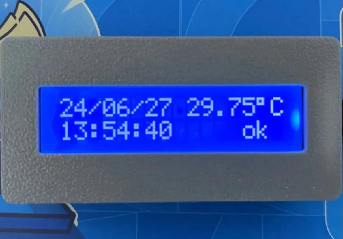
Press the SW1 button to enter the time setting calibration mode, the time on the LCD1602 LCD screen will flash to show the position of the current selected set time, press the SW2 button, add 1, press the SW3 button, minus 1, after completing the setting, you can press SW1 to move to the next set position, the order is "year→month→→ → minutes → seconds →ok", when flashing 🆗 display, click the SW2 or SW3 button to exit the setting mode and complete the time calibration setting.
 Fig.6-1 Working diagram of a simple LCD1602 temperature electronic clock
Designed by 立创EDA课程案例推荐 (from OSHWHub)
Link:https://oshwhub.com/course-examples/dan-pian-ji-ji-yu-51-dan-pian-ji-de-lcd1602-dian-zi-shi-zhong
Design Drawing
 Empty
Empty
Comment