

 Completed
[ MCU ]ESP32 minimum system board project
PRO [ MCU ]ESP32 minimum system board project
License
:Public Domain
Description
1. General overview
ESP32-WROOM-32E-N8 is a module designed by Espressif Systems in China, according to which the smallest system board is designed, all IO pins are drawn, OLED displays, buttons and three-color lamp peripherals are added, and C/C++/MicoPython can be used for development, which is convenient for quick development and learning, compact and exquisite, and has complete functions.

Fig.1-1 3D model of ESP32 minimum system board
1.1. Pin distribution

Fig.1-2 Pinout diagram of the ESP32 minimum system board
1.2. Onboard resources

Fig.1-3 ESP32 minimum system onboard resources
- Main control chip: ESP32-WROOM-32E-N8 module
- Power interface: TYPE-C
- Function buttons: reset button and BooT button
- Display function: power indicator display, two three-color light display, four-wire OLED screen display
- Debugging interface: CH340 serial port debugging
- External pins: full-featured pins are led out to facilitate the expansion of connections;
1.4. Advantages and characteristics

Fig.4-1 Minimum system board dimensions
- The appearance of the board is small and exquisite, with a size of 50mm*74mm (1968.5mil/2913.4mil);
- Support the use of C/C++/MicoPython language development, convenient for quick start learning;
- Provide TYPE-C serial port for easy development and debugging;
- On-board reset button and BooT button;
- Support 2.5GWiFi and BT/BLE wireless communication;
- It has two three-color lights and a four-line OLED display to meet the development and learning of beginners;
- Use JLC high-quality PCB and genuine components of LCSC to ensure product quality;
2. Introduction to the main controller
2.1, ESP32-WROOM-32E-N8 module introduction

Fig.2-1 Schematic diagram of the module
- Built-in ESP32-DOWD-V3 chip, Xtensa dual-core 32LX6 microprocessor, supporting up to 240Mhz clock frequency.
- 448KB ROM
- 520KB SRAM
- 16KB RTC SRAM
- N8 represents the built-in 8M Flash of the module
- Working voltage/power supply voltage: 3.0~3.6V
- PCB on-board antenna
- Integrated traditional Bluetooth BT, Bluetooth Low Energy BLE and Wi-Fi
2.2. Internal circuit diagram of ESP32 module

Fig.2-2 Schematic diagram of the internal circuit of the module
2.3. Precautions for module schematic
- In order to ensure that the power supply of the ESP32 chip is normal when it is powered on, an RC delay circuit needs to be added at the EN pin, which is usually recommended to be R=10K and C to 1uf. The specific values are adjusted according to the power-on timing of the module power supply and the power-on reset timing of the chip.
- The maximum working voltage of the module is 3.6V, and it cannot be directly connected to 5V for power supply.
- GPIO34~39 are only input pins, these pins do not have built-in pull-up or pull-down resistors, and they cannot be used as outputs.
- ESP32 has 5 strapping pins, IO12, IO0, IO2, IO15, IO5, where IO5 and IO15 start must be high, IO12 must be low, these modules have been set, can not be forced to change the state through the external pull-up or pull-down resistor, otherwise it will lead to normal start-up.
- The supply current of the external power supply needs to be at least 0.5A, and it is not recommended to use a low-current LDO drive module.
2.4 ESP32-WROOM-32E-N8 module product introduction

- Brand: ESPRESSIF
- Manufacturer model: ESP32-WROOM-32E-N8
- SKU: C701342
- Encapsulation:SMD,18x25.5mm
- Data sheet:downloading file
- Gross weight: 2.49 grams (g)
- Packing: Taping
- Purchase link: Purchase link of LCSC
3. Engineering design
3.1. Power supply circuit
The ESP32-WROOM-32E-N8 module needs 3.3V voltage supply. The power supply uses TYPE-C interface to input 5V, and then outputs 3.3V to the chip through AMS1117 step-down chip. The maximum output current of AMS1117 is 1A, which is enough to meet the power supply requirements of the module.

Fig.3-1 Power supply circuit
3.2. Main control circuit
Extend all available pins of the ESP32-WROOM-32E-N8 module and add 100nf filter capacitor to the power input part of the module to provide stable power input for the module.

Fig.3-2 Main control circuit
3.3 Serial port download circuit
Through the TYPE-C interface, the CH340 serial port chip and module communicate and download the program, because the ESP32 chip has different boot modes, the function of automatic download is realized by using two transistors, and there is no need to manually switch the level to enter.

Fig.3-3 Serial port automatic download circuit
3.4 Four-wire OLED screen interface circuit
Connect with the OLED screen through the 2.54*4P female header, add a 4.7K pull-up resistor on the IIC data bus, and add a 100nf capacitor to stabilize the power supply in the power input part.

Fig.3-4 OLED display interface circuit
3.5. RGB three-color lamp circuit
Two RGB tri-color peripherals are added, which can be used as a simple test of the module.

Fig.3-5 RGB tricolor lamp circuit
3.6. Button circuit
Lead out a reset button and a BOOT button, the BOOT button can be used as an ordinary button after the module is started normally, and the RC delay circuit is added to both buttons to complete the key debiting, and it provides a simulation for the start timing of the EN pin.

Fig.3-6 Key circuit
3.7. Expand the interface circuit
Through two 2.54*12P pin headers, all the available interfaces are drawn, and 2.54*2P pin headers are added to expand the power supply part, which is convenient for subsequent projects.

Fig.3-7 Extended interface circuit
3.8. SCH_ESP32 the smallest system board

Fig.3-8 Overall schematic diagram
3.9. PCB layout suggestions

Fig.3-9 PCB layout
- The main control module is placed in the middle of the board frame, and the antenna should not be placed in the board frame to avoid interference.
- With a certain space capacity, the OLED display is connected through the female row, and the screen printing on this side of the display screen only prompts the size and the position of the screws around it, and the components can be placed inside the screen print.
- The expansion header is placed on both sides, taking care to leave a position for the silk screen.
- Place screw holes around the screw holes, and at the same time, place a prohibitive copper pouring area around the screw holes to place a short circuit.
- The filter capacitor is placed nearby, and the power supply must first pass through the capacitor and then to the chip.
3.10 PCB wiring suggestions

Fig.3-10 PCB wiring reference diagram
- The power cable is set to 30mil, because the ESP32 module requires a large current, and the signal line can be 10mil.
- It is mainly based on the top-level wiring, and if it is impossible to go through or needs to go around for a long time, it will be switched to the bottom layer through vias.
- In the process of wiring, give priority to straight lines, do not trace at right angles or acute angles, horizontally and vertically, and symmetrically route to maintain the beautiful design.
- During the wiring process and after the wiring is completed, the GND vias are appropriately placed for heat dissipation and to ensure that the return path of the current is as short as possible.
3.11 Silk screen printing copper laying suggestions

Fig.3-11-1 Top layer of copper pouring

Fig.3-11-2 Copper pouring on the bottom layer
- Add silkscreen logo buttons and external pin information;
- After drawing and adjusting the PCB, add a teardrop effect to make the board more beautiful and stable;
- Add JLCJLCJLCJLC under the component to specify the custom editing position, and the board is beautiful;
4. Programming development
4.1. Selection of development environment
ESP32 can be developed using MicoPython/C/C++ language, Thonny IDE is recommended for development in MicoPython language, and Arduino IDE is recommended for C++ language development. It is recommended to use VScode+IDF plug-in for C development.
4.2. Download the program
In addition, if you want to download someone else's firmware, you can use Espressif's official flash programming tool, which I will place in the attachment.

Fig.4-2 Downloading the tool
5. Physical verification
5.1 Bill of Materials
| serial number | name | device designation | parameter | quantity | encapsulation | Item number |
| 1 | TYPE-C interface | USBC1 | TYPE-C-31-M-12 | 1 | USB-C_SMD-TYPE-C-31-M-12 | C165948 |
| 2 | resistance | R5、R1、R4 | 1K | 3 | R0805 | C17513 |
| 3 | R2、R3 | 4.7K | 2 | C269746 | ||
| 4 | R6、R7、R8、R9 | 10K | 4 | C17414 | ||
| 5 | LED lights | LED3 | 红灯 | 1 | LED_0805 | C84256 |
| 6 | LED1、LED2 | RGB tri-color light | 2 | LED-ARRAY-SMD_4P-L1.6-W1.5-BR_XL-1615RGBC-RF | C965840 | |
| 7 | capacitance | C2、C4 | 10uf | 2 | C0805 | C15850 |
| 8 |
C3、C5、C1、C6、C7、C9、C8 |
100nf | 7 | C38141 | ||
| 9 | Buck chips | U1 | AMS1117-3.3 | 1 | SOT-223-3_L6.5-W3.4-P2.30-LS7.0-BR | C6186 |
| 10 | Row mother | U2 | 2.54*4P | 1 | OLED-TH_L27.8-W27.2-P2.54_C9900033791 | C5248080 |
| 11 | SMD buttons | SW1、SW2 | Two-pin patch buttons | 2 | Key_SMD_3.6x6.1x2.5 | C118141 |
| 12 | Serial port chip | U3 | CH340C | 1 | SOP-16_L10.0-W3.9-P1.27-LS6.0-BL | C84681 |
| 13 | ESP32 module | U4 | ESP32-WROOM-32E-N8 | 1 | WIFI-SMD_ESP32-WROOM-32E | C701342 |
| 14 | Pin header | H1、H2 |
2.54*12P |
2 | HDR-TH_12P-P2.54-V-M | C2840012 |
| 15 | H9、H6、H8、H7 |
2.54*2P |
4 | HDR-TH_2P-P2.54-V-M-1 | C124375 | |
| 16 | Transistor | Q1、Q2 |
SS8050 |
2 | SOT-23-3_L2.9-W1.3-P1.90-LS2.4-BR | C2150 |
5.2. Device welding
On the PCB editing page of JLC EDA professional board, select the tool and open the soldering assistant tool to help quickly locate the device position.

Fig.5-2-1 Top-layer welding

Fig.5-2-2 Bottom layer welding
Welding precautions
- Weld TYPE-C first, and make sure that TYPE-C is not shorted before welding others.
- After the SMD device is soldered, the plug-in pin header is soldered.
- Before soldering the chip, use a multimeter to measure whether there is a short circuit and place the burned-out chip.
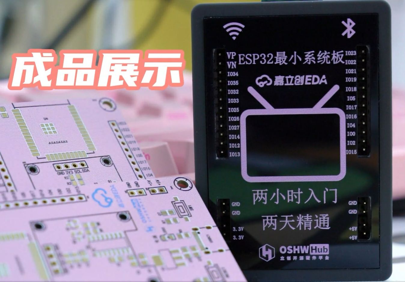
5.3. Finished product display
Designed by 立创EDA课程案例推荐 (from OSHWHub)
Link:https://oshwhub.com/course-examples/dan-pian-ji-esp32-zui-xiao-xi-tong-ban-xiang-mu
Design Drawing
 Empty
Empty
Comment