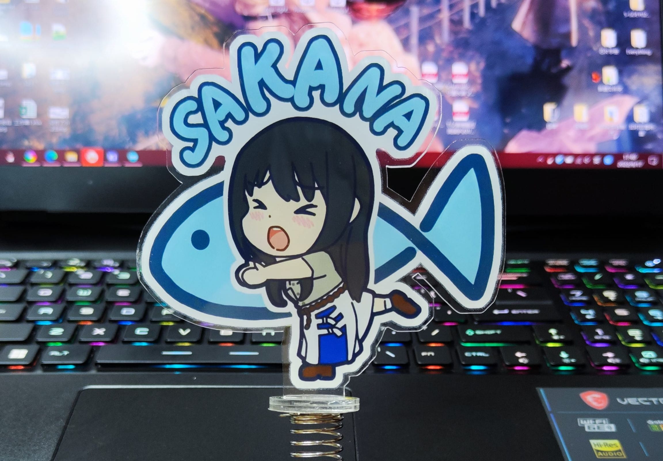
 Completed
JLC panel printing |SAKANA~
PRO JLC panel printing |SAKANA~
License
:GPL 3.0
Description
If the digital voice is played suddenly, it means that it is too sensitive to switch to the internal space of the chip, and the 1.4K resistor should be changed to 1.5K, or the 22uf capacitor should be changed to 10uf.

Brief introduction
- Soldered and ready to use, no need to burn or install any software driver.
- Use the LC panel printing service, you can get 4 stands at a time, the thickness of the board is 1.5mm, the single character stand card is 100X100mm larger than Taobao, the file is in the professional version of the editor, click the order button to place an order directly, https://dos.szlcsc.com/
- Use Taobao cost-effective audio playback chip (CH8001)
- 100mah lithium battery, USB & battery automatically switch power supply, with music switch to avoid social death.
- External FLASH, plug in USB can simulate the U disk to easily update the audio, only a USB cable can also be used as a player.
- Because of the use of the built-in direct push function, the sound quality can be heard, and you can add the amplifier core to the drawing board by yourself to use the DAC output mode.
- Demo video: https://www.bilibili.com/video/BV1uN4y1K7j4/
![]()
Assembly & Welding Instructions
- The round base plate under the character stand is stacked on top of each other and fixed to the rocker spring with UV glue.
- 3 magnets need to be installed inside the printed magnetic lid to hold the rocker spring.
- The PCB is fixed with 2 self-tapping screws.
- Middleware installation needs to pay attention to the direction.
- The housing assembly will be very tight for the first time, and it will gradually become loose after several disassembly and assembly, and then install the PCB, battery and speaker.
- The soldering chip vibration switch is not resistant to high temperature and is easy to break, so it is necessary to pay attention to the temperature not to be too high for too long, within 300 degrees for 1 second.
Special materials
- Voice chip CH8001
- Rocker springs
- Self-tapping screws M1.2x4
- Lithium battery 401119
- Shock switch
- Φ20 horn
- Φ8 2mm thick magnet, no other special requirements to buy casually.
Print instructions
FDM:
The printing middleware can not have elephant feet, and if there is, it needs to be polished off.
Due to different printers and different brand materials, the printing effect is slightly different,so two assembly clearances were made, tight and loose.
Print tightly first, and increase the amount of extrusion if it is still loose when it is tightly punched.
Light-curing:
I haven't tried it yet, and I feel that the application assembly is tighter to print.


Designed by 甘草酸不酸 (from OSHWHub)
Link:https://oshwhub.com/jie326513988/sakana-yu-yin-bo-fang-qi
Design Drawing
 The preview image was not generated, please save it again in the editor.
 Empty
Empty


Comment