

 Completed
JBC-C210-USB temperature control welding pen
PRO JBC-C210-USB temperature control welding pen
License
:CC BY-NC-SA 4.0
Description
Foreword: A long time ago, when I first took the electric soldering iron for soldering, I thought about a question, why the electric soldering iron is so long now, and the soldering is a little shaky, and then it is so long, and the shaking is even worse, and the volume is not easy to carry, and the heating and preheating are slow. I just want to make my own small and convenient soldering iron.
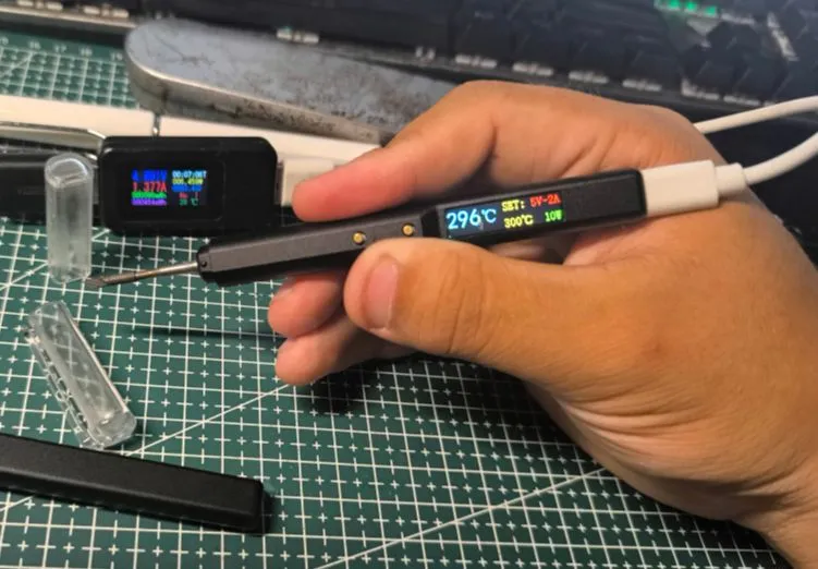
This is an ultra-small digital display temperature control welding pen, 3 seconds tin, automatic temperature control, full-color digital display, ultra-small size. The size is even slightly smaller than a regular gel pen.

It is recommended to use imported JBC-C210 for the soldering core. Domestic C210 is also available.
Basic parameters:
Power supply:type-c(5V-2A)
Power:10W
Temperature rise speed: 3~4S(5V-2A 300°C)
Open source license: CC-BY-NC-SA-4.0 (commercial use is strictly prohibited, infringement must be investigated)
Workflow Block Diagram:

Master Selection: STC8H8K64U-QFN32 (Program Running IRC Frequency 11.0592MHz)

Here, in order to reduce the size of the circuit board as much as possible and compress the space, QFN-32 is selected for the package.
Remarks in the development process: At the beginning, I planned to use the STC32G12K128 model, C251 programming, but later the test found that in the case of C251, it will be very limited to write the TFT swipe program, (compatibility error) and then downgrade and replace STC8H at the beginning without noticing the pins, When downgrading from STC32G to STC8H, pay attention to the P1.2 pin, the two chips are not the same, and in the STC8H-QFN32 package, the program cannot set this pin as the output, if it is set as the output, the chip will not be able to boot. In order to facilitate debugging, the program downloads and communicates directly with the computer through P3.2 to enter the USB download mode (download button on the board).
Temperature control selection MAX6675: (also to save space, eliminating the analog peripheral circuit, but at the cost of low temperature sampling speed)

In order to avoid the MAX6675 thermocouple temperature measurement pin backfilling high voltage and causing the MAX6675 to burn, it is necessary to add a buffer clamp circuit on the T+ signal line to limit the maximum voltage of the pin (MAX6675 all pins can withstand 3.3V) The heating period on the program is not measured, and the temperature measurement period is not heated, these two points must be staggered! In addition MAX6675 the temperature conversion process requires about 200ms conversion time, (here you need to ensure that the time of each conversion of temperature data in the program is not less than 200ms, otherwise the data will not be released)
The single-chip microcomputer asked the temperature of the MAX6675, but before the MAX6675 finished calculating the temperature, the single-chip microcomputer asked again, and then MAX6675 and recalculated, and it was for this reason that the data was not produced at the beginning.

Process: Heat for a period of time, power off, wait for discharge, measure the temperature to determine whether it is necessary to continue heating, yes: continue heating, no: stop heating.
The heating time is also used as the conversion time of the MAX6675 to the last temperature data, which improves the efficiency of the program.
About the soldering iron heating core:
I can't find the information of JBC-C210 on the Internet, there is no information at all, and I also accidentally found that the C210 soldering core is domestic.
But there is still no information, and then I bought two heating cores online to measure the pin definition, and mapped out the 3D modeling of the soldering iron core according to the physical map for assembly and design simulation, (see the attachment for the modeling file)

After three changes to the board, the pin definition was measured (I don't know if it's right, if you have information, you can reply in the comment area)

About the screen:
The screen is 0.99-inch SPI interface TFT-LCD screen (control chip GC9D01), resolution 40*160 RGB full color.

Note:Middle number 6 That area is a screen dead pixel,It has nothing to do with the program display,(I'm very lucky,I bought two screens during the test,One screen was broken because of too many bends,One screen has a dead pixel on the power)The new one hasn't arrived yet,You can only test it with a dead pixel first.
When buying the screen, choose the plug-in model, and plug in the wire with the gold finger facing up.


There's nothing to say about the circuit.,It's also connected and can be used (here the backlight circuit I reserve.,After the follow-up upgrade program can be written to sleep)
Screen Links:

The value of R38 resistance affects the maximum brightness of the backlight, and the lowest value cannot be lower than 10Ω, which is too low and has the risk of burning.
About the buttons:
It is important to note here: LC number: C318886 (only the height of the keys of this model is enough, and the height of the keycaps of many models I bought before is not enough)


Download button (SW3) without soldering:

About PCB:
At the beginning, the first version considered the current carrying reasons and wanted to do power detection and fast charging, the design was a 4-layer board, but the actual cost was relatively high, and the measured wiring voltage drop was large (the subsequent consideration of the wiring thickening, and change the scheme), the second version cut off the non-essential functions, and optimized the circuit and wiring, and successfully changed to a 2-layer board, when PCB proofing, pay attention to the board thickness must choose 0.8mm board thickness, otherwise the shell can not be installed.


About the shell:
Housing Body:
The shell is an aluminum alloy shell, which needs CNC machining, and 3D printing is not available here, and the temperature of the heating core of the electric soldering iron will melt the 3D printed parts in the working state!
Shell processing: The shell is CNC machining for JLC.
The process parameters are: aluminum alloy -6061GB/T 1804-2000 m grade Ra3.2.
The surface treatment is: ordinary anodized - black - matte (not required here, can be individually selected)

The shell is modeled in Solidworks.


Processing of pen caps:
I use JLC SLA resin to print the pen cover, but the measured resin structure strength is not enough, if it is a version with a hook, the hook itself is fragile, but the cost of 3D printing is low.
It is recommended to use high-temperature resistant and transparent materials, 3D printing or CNC machining.


The pen cap can also be used as a simple soldering iron holder when used in ordinary use.
Overall assembly simulation drawing:


Physical Drawing:


In turn:
The initial default temperature after booting is 300 degrees Celsius (the default temperature program can be changed, but it is not recommended to exceed 400 degrees)
+ button once to press temperature +10 - button to press once temperature -10.
Follow-up upgrades and improvement directions:
1. In the case of not increasing the volume, add PD and QC fast charging protocol support.
2. The maximum power is increased from 10W to 100W.
3. Optimized the UI interactive interface and added real-time power change display.
4. Stay tuned
The 3D shell and program files are attached:
Designed by 模成Electron (from OSHWHub)
Design Drawing
 Empty
Empty
Comment