

 Completed
Handheld laser measuring instrument
PRO Handheld laser measuring instrument
License
:Public Domain
Description
1. Project introduction
This project uses domestic chips, GigaDevice's GD32F303CBT6 as the main control chip, uses TYPEC interface for power supply, and adds lithium battery charging and discharging circuit and power switching circuit to ensure portability of use, using VL53L0x laser measurement sensor, which can achieve accurate measurement within 2 meters, trigger measurement by pressing buttons, OLED screen display measurement data, and buzzer to remind.
2. Onboard resources

- Main control chip: GD32F303CBT6;
- Power interface: TYPE-C 6Pin;
- Display interface: 4-wire OLED display interface, battery charging indication LED, power indicator;
- Boot mode: BOOT mode configuration, resistance welding;
- Debugging interface: SWD programming mode, 4Pin in-line pin header;
- Debugging interface: SWD programming mode, 4Pin in-line pin header;
3. Advantages and characteristics

- The board has a slender appearance and is easy to hold with one hand, and the size is 40mm*99mm (1574.803mil*3897.638mil);
- The overall layout is not compact, which is convenient for welding;
- The chip and each sensor are cheap, rich in functions and cost-effective;
- Use high-quality PCB and genuine components to ensure product quality;
4. Circuit analysis

Fig.4-1 Schematic diagram of a handheld distance measuring instrument
1. Power supply circuit
The power supply circuit is mainly composed of TYPE-C power supply circuit, power switching circuit and LDO-5V to 3.3V circuit, using 6PinTYPEC interface, which is simple and convenient and easy to solder.

Figure 4-2 TYPE-C power supply circuit
LDO-5V to 3.3V step-down circuit, the power supply from TYPEC or battery, the output is 3.3V through LDO step-down, which supplies power to the main control chip, and the capacitor is the filter, so that the output voltage signal is more stable.

Fig.4-3 LDO-5V to 3.3V circuit
The power switching circuit is composed of AO34001Amos transistor and 1N5819 Schottky diode to realize the fast switching between the TYPEC interface and the lithium battery.

Fig. 4-4 Automatic power switching circuit
2. Main control circuit
GD32F303CBT6 adopts Cotrx-M4 core, has 120M main frequency, 128KFlash, 32KRAM, the capacitance here is the filtering effect, when drawing the PCB, try to be placed as close to the pins of the chip as possible, and at the same time control the BOOT0 pin through the resistor to control the boot mode, note that the BOOT pin can not float, the chip low level enters the reset, SW2 is the reset button, when the key is pressed, the reset pin is pulled down to enter the reset.

Fig.4-5 GD32F303CBT6 main control circuit
3. Crystal oscillator circuit
The function of the crystal oscillator is to provide a clock signal to the main control chip, the role of the crystal oscillator side capacitor is to ensure that the output oscillation frequency is more stable, and the 8Mhz crystal oscillator circuit provides a clock signal for the single-chip microcomputer.

Fig.4-6 Crystal oscillator circuit
4. Sensor circuit
The four-wire OLED screen is used to display the measurement data, and the module itself has a pull-up resistor, and the IIC interface can be connected without external connection.

Fig. 4-7 Four-wire OLED screen circuit
The VL53L0x laser sensor module is used for laser ranging, the module is IIC communication, and has two control pins, and the module is compatible with 3.3V and 5V levels.

Fig.4-8 Laser measurement circuit
The passive buzzer is used for measurement prompts, the NPN type transistor is used to drive the buzzer, R6 is the base limit current resistance, and R7 is used for fast shutdown and prevents the buzzer from abnormal sound caused by level confusion when powering on.

Fig. 4-9 Passive buzzer circuit
5. Lithium battery charging circuit
The TP4056X single-cell lithium battery charge and discharge chip is used to charge the lithium battery, LED2 is the charging indicator, LED3 is the charging completion indicator, and the charging current is modified by modifying the resistance value of R3.

Fig.4-10 Lithium battery charging circuit
The single-chip ADC supports a maximum of 3.3V sampling, and converts the battery voltage into the normal range through the resistor divider, so as to judge the remaining battery power.

Fig. 4-11 Battery voltage measurement circuit
6. Basic peripheral circuits
The output function of the IO of the microcontroller is tested by the LED light, and it can also be used as a status indicator.

Fig.4-12 LED lamp circuit
The input function of the microcontroller IO can be tested by pressing the button, and it can also be used as the input of the startup measurement status.

Fig.4-13 Button circuit
6. Download the circuit
Using SWD download, through the 2.54*4P female arrangement, the download pin is led out, which is convenient to connect to the external downloader.

Fig.4-14 SWD download circuit
5. PCB layout suggestions

Fig. 5-1 PCB layout reference
- The power cable is set to 30mil, and the signal line is set to 10mil;
- The device is placed on the top layer as much as possible, and the battery interface is placed on the bottom layer.
- The top-layer wiring is the mainstay, and the unreachable line can be placed via to switch to the bottom layer for connection;
- In the process of wiring, priority is given to straight lines, and the places that need to be turned are mainly obtuse angles or arcs of 135°, horizontal and vertical, so as to maintain the beautiful design;
- The crystal oscillator wiring should be as short as possible, and the bottom should not be traced to reduce noise interference;
- In the process of wiring, the GND fan hole should be appropriately placed to occupy the space to avoid the incomplete GND after copper pouring;
6. PCB layout suggestions


Fig. 6-1 Schematic diagram of copper pouring on the top layer

Fig.6-2 Schematic diagram of copper pouring on the bottom layer
- Marking the board information (hand-held distance meter)
- Add silkscreen marking buttons, external pins and debugging interface functions;
- After the drawing adjustment is completed, the teardrop effect is added to the PCB to make the board more beautiful and stable;
- Add JLCJLCJLCJLC under the component to specify the custom editing position, and the board is beautiful;
7. Device welding

Fig.7-1 Schematic diagram of welding aids
Order of reference
- First weld the TYPEC interface to ensure there is no short circuit in the power supply.
- Then weld the chip, making sure the pins are properly soldered, with no tinning or soldering.
- Then weld resistors, capacitors, diodes, chips, and crystal oscillators.
- Finally weld the switch and plug-in bar.
Precautions
- When welding, you can select the welding auxiliary tool in the EDA toolbar of JLC, which is convenient for real-time interaction;
- After soldering, use alcohol or washing water to clean the feeling, and carefully check whether there is a problem with the chip and interface;
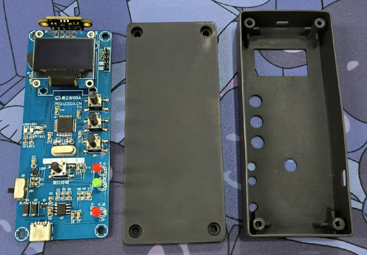
8. Physical demonstration

Fig.8-1 PCB and enclosure diagram

Fig. 8-2 Renderings
Designed by 立创EDA课程案例推荐 (from OSHWHub)
Link:https://oshwhub.com/course-examples/shou-chi-shi-ji-guang-ce-liang-yi
Design Drawing
Intellectual Property Statement & Reproduction Instructions
This is an open-source hardware project. All intellectual property rights belong to the creator. The project is shared on the platform for learning, communication, and research only; any commercial use is prohibited. If your intellectual property rights are infringed on EasyEDA, please notify us by submitting relevant materials in accordance with the Rules for Complaints and Appeals of IPR Infringement.
Users must independently verify the circuit design and suitability when replicating this project. All risks and consequences are borne by the user, and the platform assumes no liability.
 Empty
Empty
Comment