

 Completed
[ Digital circuit ]Basic logic gate discrete component circuit
PRO [ Digital circuit ]Basic logic gate discrete component circuit
License
:GPL 3.0
Description
1. Project Introduction
Logic gate is the basic unit of digital circuit, which can realize various logic relations. The basic logic gate discrete component circuit is constructed by MOS tube to realize the verification and, or, not, and not, or not, the same or and XOR logic operations.
2. Principle analysis
1.1 PMOS
PMOS refers to a MOS transistor that transports current through the flow of holes on an N-type substrate (SUB) and P-channel. Forming a conduction channel requires negative charge attraction, low level conduction, and high level cut-off.

Fig.1-1-1 Schematic diagram of PMOS symbol and structure
When using PMOS control, it is usually placed above the load as a top tube, and a pull-up resistor is often added to the PMOS to keep a stable high-level initial state to prevent the PMOS gate level from being disturbed by external interference and producing an uncertain stateto ensure that PMOS is turned off by default. When P0 is low, PMOS turns on and the LED lights up; When P0 is high, the PMOS is off and the LED is off.

Fig.1-1-2 PMOS switch control circuit diagram
1.2 NMOS
NMOS refers to a MOS transistor that transports electric current on a P-type substrate (sub) and N-channel by the flow of electrons. Forming a conduction channel requires positive charge attraction, high level on, and low level cut-off.

Fig.1-2-1 Schematic diagram of NMOS symbol and structure
When using NMOS control, it is usually placed under the load as a downtube, and a pull-down resistor is often added to the NMOS to keep a stable low-level initial state to prevent the NMOS gate level from being disturbed by external interference and producing an uncertain stateto ensure that NMOS is disabled by default. When N0 is low, the NMOS is turned off and the LED is off; When N0 is high, the NMOS turns on and the LED lights up.

Fig.1-2-2 NMOS switching control circuit diagram
1.3 CMOS
CMOS consists of PMOS and NMOS in a symmetrically complementary form, with C standing for "complementary". Low static power consumption, fast switching speed, strong anti-interference ability, high work efficiency, high integration, and superior performance.
2.1 AND gate
AND gate, also known as logic product circuit. The output is high (Logic 1) only when the inputs are all high (Logic 1), otherwise the output is low (Logic 0).

Fig.2-1-1 Logical symbols (rectangular national standard symbol and shape feature symbol).
Table 1-1 and the true value table
|
input |
output |
|
|
A1 |
B1 |
Y1 |
|
0 |
0 |
0 |
|
0 |
1 |
0 |
|
1 |
0 |
0 |
|
1 |
1 |
1 |
Logical expression: Y1 = A1·B1

Fig.2-1-2 CMOS and gate circuits
Operating principle:
(1) When A1 input is low and B1 input is low, Q1, Q2, Q5 are on, Q3, Q4, Q6 are cut-off, and Y1 is output low;
(2) When A1 input is low and B1 input is high, Q2, Q5, Q6 are on, Q1, Q3, Q4 are cut-off, and Y1 is output low;
(3) When A1 input is high and B1 input is low, Q1, Q4, Q5 are on, Q2, Q3, Q6 are cut-off, and Y1 is output low;
(4) When A1 input is high and B1 input is high, Q3, Q4, Q6 are on, Q1, Q2, Q5 are cut-off, and Y1 is output high;

Fig.2-1-3 Working schematic diagram of CMOS and gate circuit
2.2 OR gate
OR gate, also known as logic and circuitry. As long as one of the inputs is high (logic 1), the output is high (logic 1); The output is low (logic 0) only when all inputs are low (logic 0).

Fig.2-2-1 or gate logic symbols (rectangular national standard symbols and shape feature symbols).
Table 1-2 or Truth Values
|
input |
output |
|
|
A2 |
B2 |
Y2 |
|
0 |
0 |
0 |
|
0 |
1 |
1 |
|
1 |
0 |
1 |
|
1 |
1 |
1 |
Logical expression: Y2=A2+B2

Fig. 2-2-2 CMOS or gate circuit
Operating principle:
(1) When A2 input is low and B2 input is low, Q1, Q2, Q6 are on, Q3, Q4, Q5 are cut-off, and Y2 is output low;
(2) When A2 input is low and B2 input is high, Q1, Q3, Q5 are on, Q2, Q4, Q6 are cut-off, and Y2 is output high;
(3) When A2 input is high and B2 input is low, Q2, Q3, Q4 are on, Q1, Q5, Q6 are cut-off, and Y2 is output high;
(4) When A2 input high and B2 input high, Q3, Q4, Q5 are on, Q1, Q2, Q6 are cut-off, and Y2 is output high;

Fig.2-2-3 Working principle of CMOS or gate
2.3 NOT gate
NOT gate, also known as logic no circuit. When the input is low (logic 0), the output is high (logic 1); When the input is high (logic 1), the output is low (logic 0).

Fig.2-3-1 Non-gate logic symbols (rectangular national standard symbols and shape feature symbols).
Table 1-3 Non-true values
|
input |
output |
|
A3 |
Y3 |
|
0 |
1 |
|
1 |
0 |
Logical expression: Y3=A3'

Fig.2-3-2 CMOS non-gate circuit
Operating principle:
(1) When the A3 input is low, Q1 is on, Q2 is cut-off, and Y3 is output high;
(2) When the input of A3 is high, Q2 is on, Q1 is cut-off, and Y3 output is low;

Fig.2-3-3 Working schematic diagram of a CMOS NAND gate circuit
2.4 NAND gate
NAND gate is a superposition of NAND gate and NAND gate. The output is low (Logic 0) only when the inputs are all high (Logic 1), otherwise the output is high (Logic 1).

Fig.2-4-1 NAND gate logic symbols (rectangular national standard symbols and shape feature symbols).
Table 1-4 Non-true values are used in the same table
|
input |
output |
|
|
A4 |
B4 |
Y4 |
|
0 |
0 |
1 |
|
0 |
1 |
1 |
|
1 |
0 |
1 |
|
1 |
1 |
0 |
Logical expression: Y4=(A4·B4)’

Fig.2-4-2 CMOS and NAND gates
Operating principle:
(1) When A4 input low and B4 input low, Q1 and Q2 are on, Q3 and Q4 are cut off, and Y4 is output high;
(2) When A4 input low and B4 input high, Q2, Q4 are on, Q1 and Q3 are cut-off, and Y4 is output high;
(3) When A4 input is high and B4 input is low, Q1 and Q3 are on, Q2 and Q4 are cut off, and Y4 is output high;
(4) When A4 input high and B4 input high, Q3 and Q4 are on, Q1 and Q2 are cut off, and Y4 is output low;

Fig.2-4-3 Working schematic diagram of CMOS and NAND gates
2.5 NOR Gate
NOR gate is a superimposed combination of NOR gate and NOR gate. The output is high (logic 1) only when the inputs are all low (logic 0), otherwise the output is low (logic 0).

Figure 2-5-1 NOR gate logic symbols (rectangular national standard symbols and shape feature symbols)
Table 1-5 or non-true value table
|
input |
output |
|
|
A5 |
B5 |
Y5 |
|
0 |
0 |
1 |
|
0 |
1 |
0 |
|
1 |
0 |
0 |
|
1 |
1 |
0 |
Logical expression: Y5=(A5+B5)'

Fig.2-5-2 CMOS or NAND gate circuit
Operating principle:
(1) When A5 input is low and B5 input is low, Q1 and Q2 are on, Q3 and Q4 are cut off, and Y5 is output high;
(2) When A5 input low level and B5 input high level, Q1 and Q4 are on, Q2 and Q3 are cut off, and Y5 output is low;
(3) When A5 input is high and B5 input is low, Q2 and Q3 are on, Q1 and Q4 are cut-off, and Y5 is output low;
(4) When A5 input high and B5 input high, Q3 and Q4 are on, Q1 and Q2 are cut off, and Y5 is output low;

Fig.2-5-3 Working principle of a CMOS or NAND gate circuit
2.6 XNOR gate
XNOR gate can be composed of only NAND gate or NOR gate, with the same input and the output as high (logic 1) and different inputs and low output (logic 0).

Fig.2-6-1 Logical symbols of the same or gate (rectangular national standard symbol and shape feature symbol).

Fig. 2-6-2 Implementing the same or gate
Table 1-6 Table of true values of the same or the same
|
input |
output |
|
|
A6 |
B6 |
Y6 |
|
0 |
0 |
1 |
|
0 |
1 |
0 |
|
1 |
0 |
0 |
|
1 |
1 |
1 |
Logical expression: Y6=A6⊙B6=A6·B6 + A6’·B6’

Fig.2-6-3 CMOS or gate circuit
Operating principle:
(1) When A6 input is low and B6 input is low, Q1, Q2, Q3, Q4, Q6, Q9 are on, Q5, Q7, Q8, Q10, Q11, Q12 are cut-off, and Y6 output is high;
(2) When A6 input low level and B6 input high level, Q3, Q4, Q5, Q7, Q10, Q12 are on, Q1, Q2, Q6, Q8, Q9, Q11Cut-off, Y6 output low;
(3) When A6 input high level and B6 input low level, Q1, Q2, Q5, Q8, Q10, Q11 are on, Q3, Q4, Q6, Q7, Q9, Q12 cut-off, Y6 output low;
(4) When A6 input high and B6 input high, Q5, Q6, Q7, Q8, Q11, Q12 on, Q1, Q2, Q3, Q4, Q9, Q10 cut-offY6 output high;

Fig.2-6-4 Working principle of CMOS OR gate circuit
2.7 XOR gate
XOR gate consists of an AND gate, an OR gate, and an NAND gate with different inputs and an output high (logic 1) and the same input and an output low (logic 0).

Fig.2-7-1 XOR gate logic symbols (rectangular national standard symbols and shape feature symbols)

Fig.2-7-2 XOR gate implementation diagram
Table 1-7 Table of XOR true values
|
input |
output |
|
|
A7 |
B7 |
Y7 |
|
0 |
0 |
0 |
|
0 |
1 |
1 |
|
1 |
0 |
1 |
|
1 |
1 |
0 |
Logical expression: Y7=A7⊕B7=A7·B7’ + A7’·B7

Fig.2-7-3 CMOS XOR gate circuit
Operating principle:
(1) When A7 input low and B7 input low, Q1, Q2, Q3, Q4, Q8 on, Q5, Q6, Q7, Q9, Q10 are cut-offY7 output low;
(2) When A7 input low and B7 input high, Q3, Q4, Q5, Q6, Q10 are turned on, Q1, Q2, Q7, Q8, Q9 are cutY7 output high;
(3) When A7 input high and B7 input low, Q1,Q2, Q5, Q7, Q9 are on, Q3, Q4, Q6, Q8, Q10 are cut-off,Y7 output high;
(4) When A7 input high and B7 input high, Q5, Q6, Q7, Q9, Q10 are turned on, Q1, Q2, Q3, Q4, Q8 are cut-offY7 output low;

Fig.2-7-4 Working schematic diagram of a CMOS XOR gate
3. Project design
1. Schematic design
First of all, open JLC EDA, create a new project and name it [Digital Circuit] Basic Gate Discrete Component Circuit, and name the schematic file as: SCH_ Basic Gate Discrete Component Circuit.
Secondly, for device selection, all components here are selected chip devices, components can be searched in the component library of Jialichuang EDA, each component has a unique product number in the Lichuang mall, and the power interface is TYPE-C with 6PinThe female socket uses LEDs to display and verify the operation relationship of each logic gate.
Finally, the schematic diagram of the circuit is drawn, and each logic gate is drawn according to the division of the module circuit, the role of each circuit is noted, and the symbols, truth tables and expressions of each logic gate are added to facilitate understanding and learning.

Fig.3-1-1 SCH_ power input circuit

Fig.3-1-2 SCH_PMOS and NMOS circuits

Fig.3-1-3 SCH_ and gate circuits

Fig.3-1-4 SCH_ or gate circuit

Fig.3-1-5 SCH_ NAND gate circuit

Fig.3-1-6 NAND gate circuit of SCH_

Fig.3-1-7 NOR gate circuit of SCH_

Fig.3-1-8 SCH_ or gate circuit

Fig.3-1-9 SCH_ XOR gate circuit
2. Bill of materials
|
BOM_ basic logic gate discrete component circuits |
||||||
|
serial number |
name |
parameter |
tags |
quantity |
encapsulation |
Item number |
|
1 |
resistance |
10K |
R2,R5~R11,R13~R18,R20,R21,R23~R26,R28~R31, R33~R44,R46~R55 |
46 |
R0805 |
C17414 |
|
1K |
R1,R3,R4,R12,R19, R22,R27,R32,R45,R56 |
10 |
C17513 |
|||
|
2 |
capacitance |
10uF |
C1 |
1 |
C0805 |
C40894 |
|
100nF |
C2 |
1 |
C38141 |
|||
|
3 |
PMOS |
FSS2301M A1SHB |
Q1,Q3~Q5,Q9~Q11, Q15,Q17,Q18,Q21,Q22, Q25~Q30,Q37~Q41 |
23 |
SOT23 |
C2926139 |
|
4 |
NMOS |
FSS2302S A2SHB |
Q2,Q6~Q8,Q12~Q14, Q16,Q19,Q20,Q23,Q24, Q31~Q36,Q42~Q46 |
23 |
SOT23 |
C2926140 |
|
5 |
switch |
SS-3235S-L3 |
SW1~SW25 |
25 |
SW-SMD_SS-3235S-L3.00 |
C381098 |
|
6 |
LED |
红灯 |
LED1~LED10 |
10 |
LED0805 |
C84256 |
|
7 |
USB connector |
TYPE-C |
USB1 |
1 |
USB-C-SMD_TYPE-C-31-M-29 |
C2689969 |
|
8 |
Copper pillars |
M3 |
H1~H4 |
4 |
M3X10-6 |
C551322 |
3. PCB design
After completing the schematic design, after checking that the circuit is connected to the network correctly, click "Design " → "Convert Schematic to PCB" in the top menu bar (the shortcut keys areAlt+I), then save the PCB file to the project file and name: PCB_ Basic Logic Gate Discrete Component Circuit.
When drawing the frame design, it is controlled within 10cm*10cm, the border here is 10cm*10cm, add 5mm rounded corners, you can go to JLC for free proofing~
When laying out the components, all the components are placed on the top layer, and the logic gates are arranged according to the modules, and the components can be quickly placed through the "Design" → "Cross Select" (shortcut key Shift+X) functions in the top menu bar. When placing the same components, try to unify the direction as much as possible to facilitate soldering.
When wiring, the bottom line is mainly used, and the straight line is preferred, and the place that needs to be turned is mainly arc bend or obtuse angle. Once you have finished checking that the DRC is correct, add teardrops and copper pours.
Finally, add silkscreen annotation instructions to the board to make the circuit clearer.

Fig.3-2-1 PCB layout and routing reference diagram
After the top surface is drawn, the symbols, truth tables and expressions of each logic gate are placed on the back to clarify the logical operation relationship of each logic gate and facilitate understanding and learning.

Fig.3-2-2 Silkscreen appreciation of basic logic operations
4. Circuit debugging
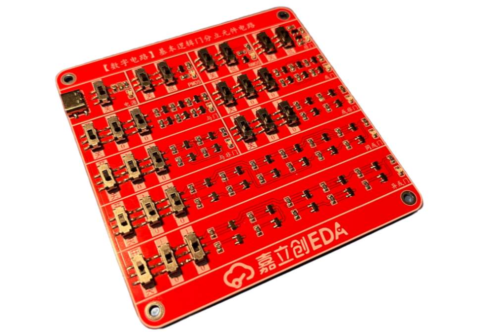
1. Device soldering
First, solder the TYPE-C interface first; second, PMOS/NMOS; Thirdly, the LEDs, resistors and capacitors, and finally the soldering switches. Note that PMOS and NMOS should not be soldered incorrectly during soldering, in each logic gate circuit, the upper left is PMOS, and the lower right is NMOS; The resistance on the LED is 1K, and the rest is 10K; The capacitor is a filter, so it can be soldered.

Fig.4-1-1 PCB assembly drawing
When welding, it can be used in JialitronClick on the welding auxiliary tool in the toolbar of EDA, and the real-time interaction is convenient for welding. Pay attention to the soldering iron tip with electric safety hands during the soldering process to avoid burns.
When soldering, the components are aligned to check whether the model is correct. The welding sequence should be carried out according to the principle from low to high to avoid affecting the welding of small components.
When the soldering chip components are clamped with tweezers, the tweezers should be removed after the solder solidifies, otherwise it is easy to cause virtual soldering. During the soldering process, pay attention to whether there is false soldering and missing soldering, so as to avoid affecting the performance of the circuit and causing the circuit to not work normally.

Fig.4-1-2 Empty PCB - top surface

Fig.4-1-3 Bottom surface of the empty PCB board

Fig.4-1-4 Physical PCBA image

Fig.4-1-5 3D rendering
2. Power-on debugging
If the welder is rough, after welding a component, you can visually check whether it is a short circuit, or you can use a multimeter to check. After the welding is completed, you need to use a multimeter to check whether the power supply is short-circuited with the ground, whether there is a short circuit and open circuit during the welding process, and the power-on test can be carried out only after the inspection is correct. It is recommended to adopt step-by-step debugging to avoid interference from other circuits.
2.1 Power Circuits
After plugging in the TYPE-C and powering on, toggle the switch to the top on, the power status indicator lights up, the power supply supplies power to the whole board, and each logic gate has an independent power switch for control, and it is recommended to control each logic gate separately when verifying.

Fig.4-2-1 Power switching circuit
2.2 PMOS circuits
Toggle on the PMOS power switch, and the PMOS circuit works normally.
- When the input level control switch is set to low, that is, the PMOS input level is low, and the indicator light is on;
- When the input level control switch is set high, that is, the PMOS input level is high, and the indicator light is off.

Fig.4-2-2 PMOS verification workchart
2.3 NMOS circuits
Toggle on the NMOS power switch, and the NMOS circuit works normally.
- When the input level control switch is low, that is, the NMOS input is low, and the indicator light is off;
- When the input level control switch is set high, that is, the NMOS input is high, and the indicator light is on.

Fig.4-2-3 NMOS verification workmap
2.4 Add gate
Toggle on the power switch with the door and the gate circuit works normally.
- When the input level control switch is set to 00, the output level is low, and the indicator light is off;
- When the input level control switch is set to 01, the output level is low, and the indicator light is off;
- When the input level control switch is set to 10, the output level is low, and the indicator light is off;
- When the input level control switch is set to 11, the output level is high, and the indicator light is on;

Fig.4-2-4 Verification with door
2.5 OR gates
Toggle the power switch on or door, or the gate circuit is working properly.
- When the input level control switch is set to 00, the output level is low, and the indicator light is off;
- When the input level control switch is set to 01, the output level is high, and the indicator light is on;
- When the input level control switch is set to 10, the output level is high, and the indicator light is on;
- When the input level control switch is set to 11, the output level is high, and the indicator light is on;

Fig.4-2-5 or Gate Verification Diagram
2.6 NAND Gate
Toggle on the NOT gate power switch, and the NOT gate circuit works normally.
- When the input level control switch is set to 0, the output level is high, and the indicator light is on;
- When the input level control switch is set to 1, the output level is low, and the indicator light is off;

Fig.4-2-6 NAND gate verification workchart
2.7 NOR gate
Toggle on the AND NOT gate power switch, and the NOT gate circuit works normally.
- When the input level control switch is set to 00, the output level is high, and the indicator light is on;
- When the input level control switch is set to 01, the output level is high, and the indicator light is on;
- When the input level control switch is set to 10, the output level is high, and the indicator light is on;
- When the input level control switch is dialed to 11, the output level is low and the indicator light is off;

Figure 4-2-7 NOR gate verification workmap
2.8 OR gate
Toggle the ON or NOT gate power switch, or the NOT gate circuit works properly.
- When the input level control switch is set to 00, the output level is high, and the indicator light is on;
- When the input level control switch is set to 01, the output level is low, and the indicator light is off;
- When the input level control switch is set to 10, the output level is low, and the indicator light is off;
- When the input level control switch is dialed to 11, the output level is low and the indicator light is off;

Fig.4-2-8 NAND gate verification workchart
2.9 XNOR gate
Toggle the power switch to open the OR gate, and the OR gate circuit works normally.
- When the input level control switch is set to 00, the output level is high, and the indicator light is on;
- When the input level control switch is set to 01, the output level is low, and the indicator light is off;
- When the input level control switch is set to 10, the output level is low, and the indicator light is off;
- When the input level control switch is set to 11, the output level is high, and the indicator light is on;

Fig. 4-2-9 Verification diagram of the XNOR gate
2.10 XOR Gate
Toggle the power switch to turn on the XOR gate, and the XOR gate circuit works normally.
- When the input level control switch is set to 00, the output level is low, and the indicator light is off;
- When the input level control switch is set to 01, the output level is high, and the indicator light is on;
- When the input level control switch is set to 10, the output level is high, and the indicator light is on;
- When the input level control switch is dialed to 11, the output level is low and the indicator light is off;

Figure 4-2-10 XOR gate verification diagram
Designed by 立创EDA课程案例推荐 (from OSHWHub)
Link:https://oshwhub.com/lceda-02/shu-zi-dian-lu-ji-ben-luo-ji-men-fen-li-yuan-jian-dian-lu
Design Drawing
Intellectual Property Statement & Reproduction Instructions
This is an open-source hardware project. All intellectual property rights belong to the creator. The project is shared on the platform for learning, communication, and research only; any commercial use is prohibited. If your intellectual property rights are infringed on EasyEDA, please notify us by submitting relevant materials in accordance with the Rules for Complaints and Appeals of IPR Infringement.
Users must independently verify the circuit design and suitability when replicating this project. All risks and consequences are borne by the user, and the platform assumes no liability.
 Empty
Empty
Comment