

 Completed
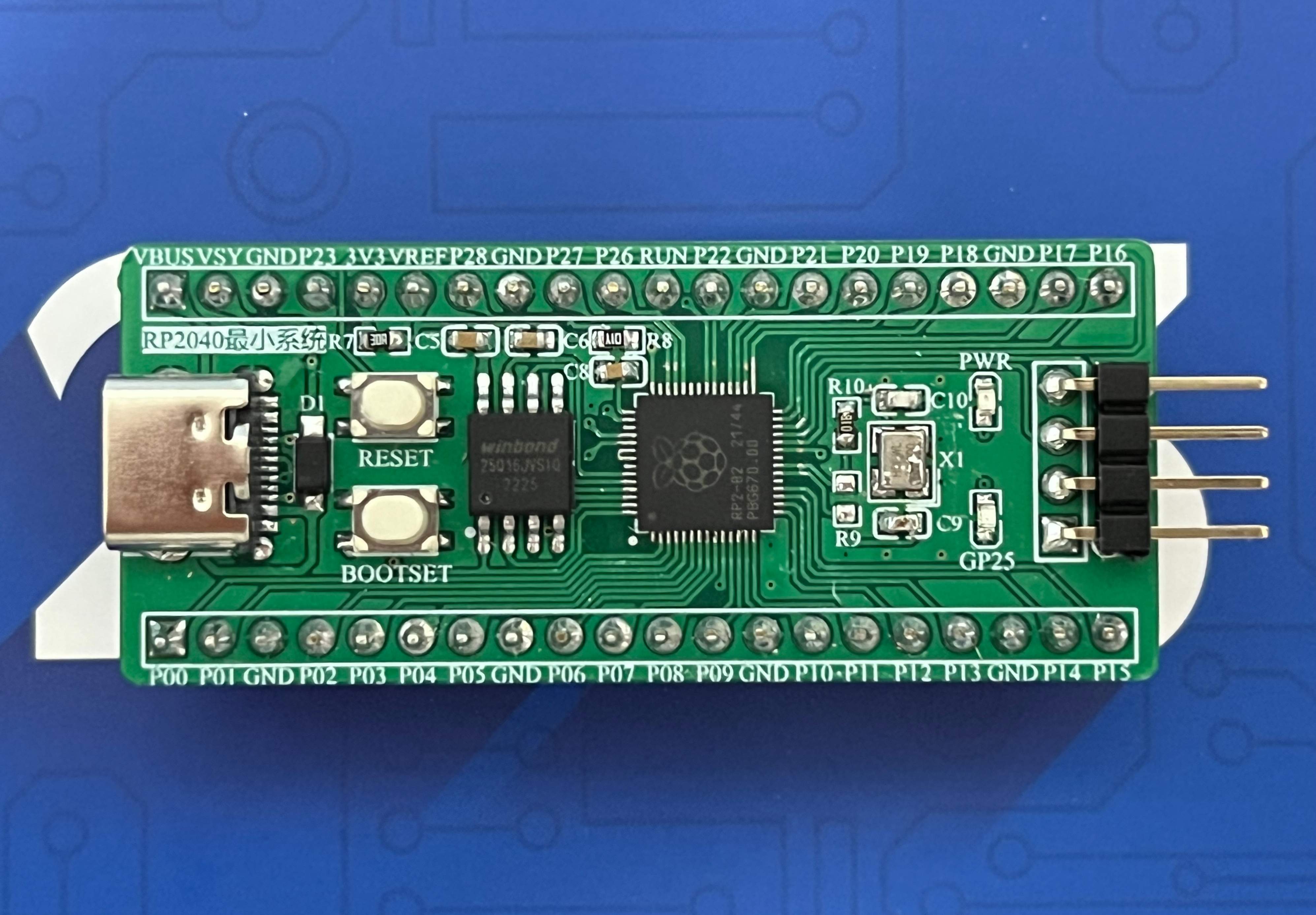
[ Core board ]RP2040 minimum system
PRO [ Core board ]RP2040 minimum system
784
0
0
0
Mode:Full
License
:GPL 3.0
Creation time:2025-02-21 03:30:34Update time:2025-02-24 02:49:22
Description
Designed by 立创EDA课程案例推荐 (from OSHWHub)
Link:https://oshwhub.com/course-examples/he-xin-ban-rp2040-zui-xiao-xi-tong
Design Drawing
Add to Album
0
0
Share
Report
Intellectual Property Statement & Reproduction Instructions
This is an open-source hardware project. All intellectual property rights belong to the creator. The project is shared on the platform for learning, communication, and research only; any commercial use is prohibited. If your intellectual property rights are infringed on EasyEDA, please notify us by submitting relevant materials in accordance with the Rules for Complaints and Appeals of IPR Infringement.
Users must independently verify the circuit design and suitability when replicating this project. All risks and consequences are borne by the user, and the platform assumes no liability.
Followers0|Likes0
Related projects
 Empty
Empty
Comment