Editor Version ×
Standard

1.Easy to use and quick to get started

2.The process supports design scales of 300 devices or 1000 pads

3.Supports simple circuit simulation

4.For students, teachers, creators

Profession

1.Brand new interactions and interfaces

2.Smooth support for design sizes of over 5,000 devices or 10,000 pads

3.More rigorous design constraints, more standardized processes

4.For enterprises, more professional users

Completed

PRO MakerLab Coke Charger 4.0 (with wireless charge)

Coke Charger 4.0 (with wireless charge)

Project tags

License

CC BY-NC-SA 3.0

License: CC BY-NC-SA 3.0

Mode:

Mode

Editors' pick

Editors' pick

  • 87
  • 0
  • 0
Update time: 2024-09-30 09:46:46
Creation time: 2024-09-30 08:31:20
Description

Description

# *Project Description* Last edited - 2023/05/04 ### Write in front * The current version of the circuit diagram is the IP5568+ chip version that supports both wireless charging input and output. It is partially different from the chip auxiliary circuit that only supports wireless charging output. * If you do not need wireless input to reproduce, use this circuit with caution (some circuit configurations are different). The IP5568 circuit without wireless input version is being drawn, and there will be many fewer components in the circuit. * If you don’t need the wireless charging function, use [Coke Power Bank 3.0](https://oshwhub.com/big_big_A/ke-le-chong-dian-bao) or [Coke Power Bank 4.1](https://oshwhub.com/hzj666888/ip5356-shuang-xiang-duo-xie-yi-kuai-chong-yi-dong-dian-yuan) |Version| Master control|Wireless charging RX|Wireless charging TX|Two-way fast charging|Mini Jar|Standard Jar|Mass Production| |:---:|:---:|:---:|:---:|:---:|:---:|:---:|:---:| |[3.0](https://oshwhub.com/big_big_A/ke-le-chong-dian-bao)|[IP5358](https://www.semiee.com/file/Injoinic/Injoinic-IP5358.pdf)|Not supported
|Not supported
|support
|support
|support
|No
| |[4.0](https://oshwhub.com/big_big_a/ke-le-chong-dian-bao-dai-wu-xian/edit)|[IP5568](https://www.semiee.com/file/Injoinic/Injoinic-IP5568.pdf)|support
|support
|support
|support
|Not supported
|No
| |[4.1](https://oshwhub.com/hzj666888/ip5356-shuang-xiang-duo-xie-yi-kuai-chong-yi-dong-dian-yuan)|[IP5356](https://www.semiee.com/file/Injoinic/Injoinic-IP5356.pdf)|Not supported
|Not supported
|support
|support
|support
|Yes
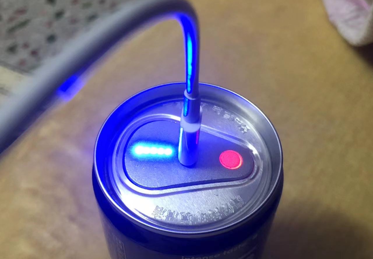
| *[Table 0]. Function support list* ## Open Source Instructions * Can be freely designed and produced according to the schematic diagram * In order to reduce the waste of JLC's resources, the remaining PCB production from proofing is allowed to be sold in small quantities to "regenerate health" * Unauthorized sale of 3D models is prohibited * Commercialization rights reserved for both PCB and 3D models ## Project Content * This project is [the fourth generation of coke charging bank series](https://www.bilibili.com/video/BV1yz4y1Y7pV) jointly developed by [MJhan](https://space.bilibili.com/94128110) of B station UP. The communication Q group of up master is: 162848318 * Inherited from the previous generation Coke Power Bank 3.0, the difference is that it uses a mini can of Coke as the casing, improved device selection, and added a wireless charging function. While having a compact and portable appearance, it also retains the two-way fast charging function; * Based on the previous generation, a new two-way wireless charging function has been added, and some component selections have been changed. Compared with the IP5358 version, it has greater improvements and has more powerful performance release. ## Related Functions * The shell is made by 3D printing, and the overall appearance is a cylindrical mini Coke can. * The shell can be produced by FDM printing or light-curing printing (the two models are slightly different, so be sure to pay attention when printing) * Small power bank based on IP5568, supports 15W wireless charging TX, 10W wireless charging RX, SCP, VOOC, PD3.0 and other common fast charging protocols * The main control has built-in battery protection, and the overall size of PCBA is about 45*45*15 * The top has an illuminated button, a two-way fast charging Type-C port, four battery indicator lights, and a fast charge indicator light. * The bottom is a wireless charging pad that supports two-way QI charging. ## Wireless Charging TX * IP5568 integrates 5w/7.5w/10w/15W wireless charging TX driver control part, which integrates two symmetrical half-bridge driver modules (drivers for upper-side PMOS and lower-side NMOS). * IP5568 integrates two ASK demodulation modules, which can collect coil voltage and current respectively for ASK communication demodulation and decoding. 1.Current decoding, directly sampling the current value for digital demodulation and decoding. 2.Voltage decoding does not require amplification. After filtering and DC blocking, it can be directly sent to the chip for digital demodulation and decoding. * IP5568 can detect the voltage and current of the coil through the built-in ADC. * When IP5568 is turned on, wireless charging will always work. * IP5568 can indicate [Table 4] wireless charging status by driving 2 LED outputs ## Wireless Charging RX * IP5568 supports wireless charging RX function, supports 5w/10w * TX and RX share a coil and a resonant capacitor, and the TX and RX modes can be switched by pressing the button (long press). * After the IP5568 is turned on, the wireless charging defaults to TX mode. * When in the wireless charging RX mode, the two LED indicators of the wireless charger will flash together to indicate that the wireless charger is working in the RX state. * When using the wireless charging RX function, the button function defaults to double-click to shut down, and there is no flashlight function. * The wireless charging RX output is directly connected to the VIN network to provide power for charging the system. * The USB charging port is preferred for system charging. When RX is working, inserting USB-B or USB-C will automatically turn off the wireless charging RX function, automatically switch to USB-B or USB-C to charge the system, and at the same time turn on the wireless charging TX function. * Using the RX solution, the button mode will be fixed to single-click to power on, double-click to power off, and long press to switch between TX and RX modes. ## Debug * The LED power display is abnormal. Check the direction of the LED. It should be positive and negative alternately. If the fault still exists after eliminating this problem, it may be that the main control chip is soldered. Try to re-solder the main control chip. * When powered on for the first time, the LED will flash quickly. Failure to discharge at this time is not a circuit problem. Just charge and activate. * Every time the main control is powered off, it needs to be recharged and activated, otherwise it cannot be used. * If the wire is too thin, it may cause the chip to report an error due to insufficient current carrying capacity (the LED indicator light flashes quickly) * Normal wired wireless charging does not take effect. It may be that the coil does not match. Try replacing the coil. * If an unknown error occurs and you cannot charge or discharge, please try the following steps. 1. You can try to re-activate after a complete power outage. 2. If the error is still reported after activation, it may be that the capacitor still has residual power. After the power is turned off again, short-circuit VSYS-GND to discharge the capacitor. 3. If the error is not resolved, it may be due to the following reasons. Please check them one by one. > The chip model does not match the circuit. If you are not sure about the model, contact the seller. > There is a short circuit or weak solder in the circuit, especially check the main control and C port. > The power cord/PCB does not carry enough current, try to replace the wire/pile tin. # Things to note when reproducing ## Material Preparation * Not all components on the BOM are corresponding to Lichuang Mall and may even be out of stock. Please check carefully before purchasing components. * Choose FR4 material for PCB proofing, and choose 1.0mm for board thickness. * The shell can be printed by FDM 3D printing or light-curing 3D printing (the two models are different) * The current carrying capacity of the connection between the battery and the PCB is up to 5A. Please pay attention to the current carrying capacity of the wire when connecting the wire (at least 1.5 square meters of copper wire) * The appearance of the cola skin is formed by digging holes in the top of the cola after drinking it and cutting off the bottom and then nesting it outside the model. > The appearance of the cola skin is formed by digging holes in the top of the cola after drinking it and cutting off the bottom and then nesting it outside the model. > The top is cut along the concave marks on the can. > Try to reserve a certain length for the bottom cut. The excess can be pressed into the model. If it is too short, it will not be fully nested. ## Welding Instructions * The battery uses four 3.7V voltage 18650 batteries. The PCB default configuration charging voltage is 4.2V. If there is a difference, the configuration resistor needs to be changed <sup>[Table 2]</sup> * The project uses IP5568+. It should be noted that IP5568 is divided into normal version and plus version. The normal version only supports wireless output TX, and the one that supports RX is IP5568+. * If you use the ordinary version of IP5568, be sure to pay attention to the differences in the circuit (there are corresponding remarks in the schematic diagram) * Due to volume limitations and current carrying requirements, the PCB needs to be additionally tinned on the back window part after the production is completed. At the same time, if the tinned part is too close, please add green oil for insulation as appropriate. * The bottom pad of the Type-C interface has very weak fixation. When welding, please be sure to add enough tin to the four corner fixing holes, otherwise it may be damaged when unplugging and plugging. * The large ground at the bottom of the chip must have enough tin, which is related to current carrying and heat dissipation. * **Welding tips** 1. Weld the front side first and then the back side. 2. Solder the chip components first, then solder the plug-in last. 3. For components that are more difficult to weld, please check for short circuit and weak soldering immediately after the welding has cooled down .(it will be difficult to find the cause of the problem if there are bugs after all is completed) 4. For devices (C port, main control) packaged in SMD or QFN, the soldering pads can be tinned first until they are completely full and not short-circuited. If there are no components, you can easily use a soldering iron to deal with the tin connection or lack of tin; there is a universal steel mesh You can also tin-plate the bottom of the chip first and then solder it. 5. Really feel their welding technology is more sorry, directly open the steel net. 6. For those who don’t want to hand-solder, there are four Mark recognition points reserved for self-installation using OpenPNP; Lichuang’s SMT is a bit expensive but really delicious! ## Assembly Instructions ### Coil Shield Cutting 1. Print the provided "coil outline.DXF" drawing with a printer at a ratio of 1:1. 2. Then stick the printed outline paper to the back of the purchased anti-interference magnet. 3. Use scissors or a cutlery to cut out the ring-shaped anti-interference tiles along the outline. 4. Finally, attach the ring-shaped anti-interference tile to the A11 wireless transmitting coil (remove the original anti-magnetic layer) *--MJhan is a hand bruiser* ### Coke cut * UP uses powerful electric grinding cutting. * A small emery saw blade was used, and then a flint grinding wheel was used for fine grinding. ![图片9.png](//image.easyeda.com/pullimage/TLoQ0A4rxtdbhrM0CSccxsn4WPlyzLkh8H6wQcCB.png) *--MJhan is a hand bruiser* `Write down the other instructions in time` # Instructions For Use `To be constructed` # Appendix ## 1.Configure The Resistor ### FCAP-battery Capacity Setting
| R8 | 25K | 40K | 50K | 60K | 100K | 125K | | :---: | :---: | :---: | :---: | :---: | :---: | :---: | |\*mAH| 5000 | 8000 | 10000 | 12000 | 20000 | 25000 |
**[Table 1].FCAP-configuration resistor for battery capacity** * IP5568 external PIN sets the initial capacity formula of the battery cell: battery capacity = R8*0.2 (mAH), the maximum support is 25000mAH * Special: FCAP retains a special function. If R8 resistance = 1K, the battery capacity defaults to 10000mAH, and the DPA2 PIN is used as the serial port print port output. * When the chip mode is RX/TX (that is, two-way wireless charging is on), the FCAP pin is reserved as a driving pin. At this time, the configuration resistor is not connected, and the battery capacity defaults to 10000mAH. * The chip has a built-in calculation function for battery capacity correction. As long as a complete charging cycle is performed (from no charge to fully charged), the battery capacity can be corrected. Therefore, there is no need to worry about errors in the capacity configuration, but be sure to pay attention. The capacity will be reset after a complete power outage and reactivation of the chip. ### VSET-Charging Voltage Configuration
| R7 | 115K | 82K | 51K | 20K | | --- | --- | --- | --- | --- | |Voltage| 4.20V | 4.30V | 4.35V | 4.40V |
**[Table 2]. Configuration resistor for battery charging voltage** * The VSET PIN is only used to set the full battery voltage when the LED power is displayed; when used in digital tube applications, VSET is used as the digital tube driver PIN. The default battery full voltage is 4.2v. This design does not use this configuration for digital tube applications. reserve * Popular science: When charging a lithium battery, it first supplies power to the battery in constant current mode. At this time, the current is constant, and the charging voltage rises as the battery power increases (reflected as the battery voltage rises); when the charging voltage reaches the threshold value (the peak value of the battery) voltage), start charging in constant voltage mode. At this time, the voltage is constant, and the current decreases as the battery power increases (the voltage difference between the battery and the power supply decreases) until it gradually approaches 0 and finally the charging is completed. ### KEY-key Mode Configuration
| R6 | Power on | Shut down | illumination | Light display | | --- | --- | --- | --- | --- | | 20K | Short press | Double click | Press and hold for 2S | LED | | 51K | Short press | N/A | Press and hold for 2S | LED | | 82K | Short press | N/A | Double click | LED | | 115K | Short press | Long press | Double click | LED |
**[Table 3]. Configuration resistor in button mode** * In the digital tube solution, KEY_MODE is used as the digital tube drive pin, and there is no key mode selection. The default button mode is: short press to turn on, short press twice in succession to turn off, and long press for 2 seconds to turn on and off the flashlight. * In the wireless charging TX/RX solution, the default button mode is: short press to turn on, short press twice in succession to turn off, long press for 2 seconds to switch between wireless charging and RX, no flashlight application. ## 2. Light Display Description ### Dual LED Wireless Indication
| state | LED_R | LED_G | | :---: | :---: | :---: | | Wireless charging abnormality (foreign objects, etc.) | bright | lights out | | Charging completed | bright | bright | | Charging |lights out | 1Hz flashing | | standby | lights out | bright |
**[Table 4]. Wireless indicator light** ### Fast charging Indicator Light * In this design, the fast charge indicator light is integrated into the center of the button, and the button also takes into account the function of fast charge indicator. * If you don’t need fast charging instructions, just replace the ordinary touch button. * HLED can indicate the current fast charging mode, whether charging or discharging. When entering fast charging mode and is in a non-5V state, the indicator light will automatically light up. ## 3.Physical Display ![PCBA俯视图](//image.lceda.cn/pullimage/GzAdaIZ9mXdWNcs9G3xZ6ALK6hrOLJxwX6pMKz28.jpeg) **[Fig.1].PCBA overall view** ![PCB+充电板](//image.lceda.cn/pullimage/YemHtNEBw40M81gqew4Io0LaSTlFxI1RZH9UszxF.jpeg) **[Fig.2].PCBA+charging board** ![三维模型](//image.lceda.cn/pullimage/AFzZCs4OLvOk3BCs2xa0tgRta4jAmYjEudBrw4q4.png) **[Fig.3]. Model preview** ![成品](//image.lceda.cn/pullimage/GK2Vul9tYj58UskZuQQ9jYa3EkVB4YtqqWD50YSC.jpeg) **[Fig.4]. Overall view of the finished product** ## 4.Video Display

Designed by AutoType (from OSHWHub)

Link:https://oshwhub.com/big_big_a/ke-le-chong-dian-bao-dai-wu-xian

Design Drawing

Design Drawing

schematic diagram
1 /
PCB
1 /
The preview image was not generated, please save it again in the editor.
Empty
Project Members

Project Members

Target complaint
Related Projects
Change a batch
Loading...

Comment

Add to album ×

Loading...

reminder ×

Do you need to add this project to the album?

服务时间

周一至周五 9:00~18:00
  • 0755 - 2382 4495
  • 153 6159 2675

服务时间

周一至周五 9:00~18:00
  • 立创EDA微信号

    easyeda

  • QQ交流群

    664186054

  • 立创EDA公众号

    lceda-cn