

 Completed
Analog signal programmed acquisition display device based on ARM-STM 32
PRO Analog signal programmed acquisition display device based on ARM-STM 32
License
:Public Domain
Description
Project Description:
Taking STM32 microcontroller as the core, a multi-channel voltage acquisition control system is designed and implemented. In order to achieve accurate collection of various analog weak signals, the system designed an ADC front-end conditioning circuit to perform program-controlled gain amplification and active low-pass filtering on the collected analog signals. Users can achieve this through program settings or external key settings. The program has multi-level adjustment of the gain. When data abnormality occurs in the collected voltage, the system can automatically alarm and automatically reduce the signal gain to prevent system damage caused by overvoltage. It has been verified that the system has the advantages of high accuracy, high reliability, and easy scalability.
Open Source Agreement
Open source agreement description.
Project Related Functions
It can collect and process 8--16 analog signals. For weak signals, the amplification factor can be controlled by program. The amplification factor is adjustable in 8 steps. For signal interference generated during the signal acquisition process, a 100Khz active low-pass filter is used. Filtering is performed to improve the reliability of data collection, and the collected and processed data are displayed through a 3.5-inch OLED. The data acquisition core is the AD7606 module, and the amplifier module is the AD8321. The data acquisition test source uses a buffered analog signal output device of LM358, and uses DDS9850 to generate waveform signals to verify the performance of the low-pass filter.
Project Properties
This project is made public for the first time and is my original project. The project has not won any awards in other competitions.
Project Progress:
2023.-3.7 Project establishment.
2.23.11.20, completed. The test results show that the data collection function is good and the basic requirements of the project have been basically completed.
Design Schematic Description:
1. The output of the module power supply is connected in parallel using magnetic beads and electrolytic capacitors, and the analog ground and digital ground are grounded at a single point through a 0R resistor.

2. The data analog signal output source is buffered with a voltage follower.

3. In order to collect a wider range of voltages, the amplifier circuit uses positive and negative power supplies.

4. Amplification circuit: Adjust the amplification factor by changing the gain resistor of AD8421.

5. Gain adjustment circuit: Use an analog switch composed of ADG708 to select the resistance value.

6. Gain indicator circuit to prompt the current gain status.

Software Description:
The core program is mainly in the folder known by the arrow.

Software tip: The software can be nested using code blocks. There is no need to explain all software parts, only the important parts are required.
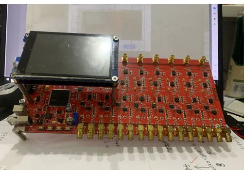
Physical Display:
①Core control panel:


This board is responsible for collecting analog signal data input from the outside, processing it, and displaying it through OLED. The gain of the collected signal can be adjusted through the program, and the gain range is adjustable multiple times.
②Analog signal output board:

This board mainly generates analog signals within +5V. The voltage amplitude of the generated signal is related to the supply voltage. By adjusting the potentiometer knob, the voltage output data is changed to achieve the verification effect.
③Low-pass filter circuit test source:

This module uses AD950 as the core output waveform, mainly to test the performance of the low-pass filter circuit. By outputting a sinusoidal signal higher than 100Khz, the waveform of the output signal is viewed through an oscilloscope to verify the performance of the low-pass filter.
④Test:


Design Considerations
A variety of analog circuits are protected in this project. Please see the schematic analysis for details.
For the zero-adjusting terminal (potentiometer) of the collected signal, this circuit can be removed according to actual needs. During the actual test process, whether the zero-adjusting terminal has little impact on the output data.
All modular PCBs in the project engineering files are verified for use.
In the actual acquisition process, when the gain is 1, the LCD display voltage is basically the same as the data collected by the multimeter, and the error is very small.
Tip: Here are some precautions that need to be paid attention to in the production of the work (if not, you can leave it out)
Other
https://www.bilibili.com/video/BV1Hu411F7Qu/
Demonstration video: You can upload the attachment to the demonstration video. Attachments can only be long-distance transferred files of up to 50M. Files larger than 50M can be placed on other network disks or video websites. Just put the address link here.
Project attachments: Works participating in the event must upload project-related program attachments to the open source platform or personal code storage cloud. The attachment can be uploaded up to 50M (please do not upload it in the Lichuang workspace, there are restrictions)
Designed by Circuit test laboratory of Shanghai Jiaotong University (from OSHWHub)
Link:https://oshwhub.com/circuit-test-laboratory/ji-yu-ARM-STM32de-mu-ni-xin-hao-
Design Drawing
Intellectual Property Statement & Reproduction Instructions
This is an open-source hardware project. All intellectual property rights belong to the creator. The project is shared on the platform for learning, communication, and research only; any commercial use is prohibited. If your intellectual property rights are infringed on EasyEDA, please notify us by submitting relevant materials in accordance with the Rules for Complaints and Appeals of IPR Infringement.
Users must independently verify the circuit design and suitability when replicating this project. All risks and consequences are borne by the user, and the platform assumes no liability.
 Empty
Empty
Comment