

 Completed
Adjustable positive and negative high voltage power supply based on STC8H8K64U
PRO Adjustable positive and negative high voltage power supply based on STC8H8K64U
License
:MIT License
Description
Project Description:
*High voltage and low current programmable DC power supply.
*Two outputs, each with independently configurable positive and negative power rails.
*Parameters can be set by joystick and knob.
*Parameters can be set through two RS232 serial ports.
*Regulated current limiting, stabilized current limiting output.
*Output with self-recovery insurance.
*All communication ports are fully isolated.
Key Parameters (Significant Digit Table Accuracy)
*Positive rail voltage 0~100.0V.
*Negative rail voltage: -100.0~0V.
*Maximum current output capacity 10.000mA.
Use
It can be used as a simple source meter, rough measurement of voltammetry characteristic curve, testing glow tubes, electron tubes, electrotherapy instruments, etc.
Open Source Description
Design ideas
*1 high-voltage isolated power supply, accepts 12V input, outputs -100V, 0V, 100V.
*Two 5V isolated power supply channels are supplied, with most circuits using -100V as the reference ground (hereinafter referred to as the low side) and a small number of circuits using 0V as the reference ground (hereinafter referred to as the high side), and the two parts can be isolated for communication.
*Use STC advanced PWM controller to output complementary PWM, followed by 2-fold RC low-pass filtering to output low ripple analog (v0.0.2 has been abandoned, because the PWM frequency does not go up, there is still more obvious ripple, changing the RC filter parameters will affect the response speed)
*Uses MS5614T 4 12-bit DAC chips to output analog.
*Proportional conversion from low voltage to high voltage using the HV264 using the HV op amp, using the default gain of 66.7.
*High-voltage level clamping with fast recovery diode, followed by heel current expansion.
*Using the INA281 for current measurement, the chip withstands only 110V common mode voltage, so two are placed on the low side and two on the high side.
*An eight-pin sub-MCU: STC8G1K08A is added to the high side for reading the high analog quantity, and communicates with the main MCU on the low side through the isolated serial port.
*The intersection of high and low voltage is slotted as much as possible to ensure good electrical isolation.
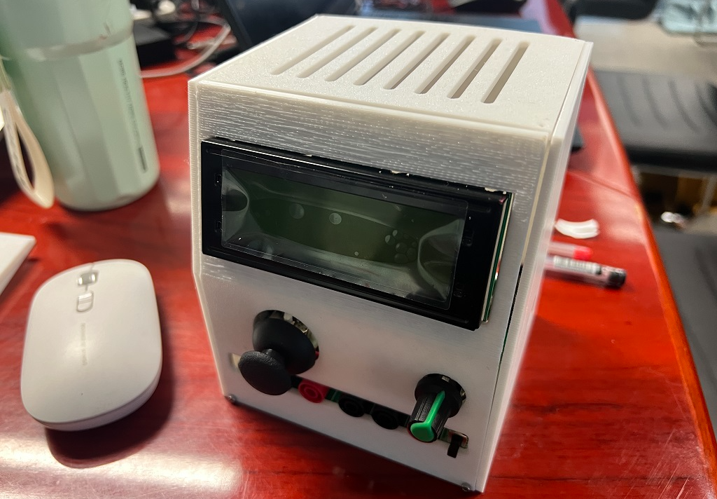
Photographs of the real thing
2024/08/12 update: v0.0.2 SMT proofing


Physical video
See annex.
(Currently using serial port command control, access to joystick and rotary encoder, with load test, and complete video after mounting the enclosure to be filled)
Some documentation of the simulation process


v0.0.2 Update (2024/08/12)
*Improved code folder organization structure to be more standardized.
*Fixed several issues with v0.0.1.
*Switch to DAC chip output analog.
*Layout has been tweaked a bit.
There is an issue with v0.0.1
1. The isolated USB cannot be downloaded in USB-ISP mode.
Temporary solution: download the cable and serial port.
TODO: In addition, check the board to verify the USB download, and add the data cable to the pull-down appropriately.
2024/08/12 update: v0.0.2 reserved D+ and D- pull-down resistor pads on the back
2. The CJ431 reference output voltage problem (expected 3.05V, actual 2.70V) is inconsistent with the simulation results
TODO: Separately check the board
Update 08/12/2024: v0.0.2 Changed to LDO to provide reference voltage
3. P3.2 The switching level is inverted (usually low, pressed high, contrary to expectations) and no stabilization
Temporary solution: Make INT0 interrupt the response to the rising edge, and the software delay debites
TODO: corrects the schematic diagram and adds an anti-shake capacitor.
Update 08/12/2024: v0.0.2 fixed
4. STC power failure download switch can not be blacked out, reason: ARIF backfilling.
TODO: Change CJ431 input to controlled MCU_VCC
Update 08/12/2024: v0.0.2 has been fixed and 3v3 LDOs also use controlled power supplies.
This is the first time I use STC microcontroller, 51 core microcontroller for project design, my software background, mold power is not solid, and time is pressing, there are many mistakes in the design, please give me more advice, thank you!
Designed by haofanurusai_2 (from OSHWHub)
Design Drawing
Intellectual Property Statement & Reproduction Instructions
This is an open-source hardware project. All intellectual property rights belong to the creator. The project is shared on the platform for learning, communication, and research only; any commercial use is prohibited. If your intellectual property rights are infringed on EasyEDA, please notify us by submitting relevant materials in accordance with the Rules for Complaints and Appeals of IPR Infringement.
Users must independently verify the circuit design and suitability when replicating this project. All risks and consequences are borne by the user, and the platform assumes no liability.
 Empty
Empty
Comment