

 Completed
PEX8796_PCIE_GEN3_24PORT_Switch
PRO PEX8796_PCIE_GEN3_24PORT_Switch
License
:GPL 3.0
Description

Project Description
The previously expensive PEX8796 has become cheap due to the popularity of PCIE4.0 5.0. However, for junkies, 96 PCIEs and a maximum of 24 ports are still very attractive. In conjunction with JLC's 6-layer hole-in-the-disk design, a cheap PEX8796 solution is designed. Whether it is multi-graphics card computing or multi-NVME expansion, mothers no longer have to worry about insufficient PCIE numbers on the computer!
Open Source Agreement
GPL3.0
Project Related Functions
PCIE3.0X16 connects to the computer as the upstream, 80 PCIE3.0 as the downstream, 80 PCIE through the dip switch, any combination of X16,X8,X4 multiple split states!
Detailed Review Article
20x NVMe! KCORES PEX8796 PCIe Switch super expansion card unboxing test - bilibili (bilibili.com)
Detailed Drawing Board Video
(PEX8748 and PEX8749 have the same design, except that PEX8748 is smaller and designed in the same way)
[Use JLC EDA to rub PLX8748 online]-1. Selection and layout_bilibili_bilibili
Project Properties
This project is made public for the first time and is my original project. The project has not won any awards in other competitions.
Project Progress
PEX8796 has been verified to be OK and operates normally. This card has PCIEX16 3.0 input and 80 PCIE 3.0 outputs. The 80 PCIE 3.0 can be any combination of X16, X8, and X4. At this point, all kinds of weird things will definitely pop up.
For example: If you don't feel satisfied with running, of course you won't be satisfied with running. If you think it's not enough, of course you won't use it.
Why can it be divided into so many monsters? (Similar to the way your Nanqiao works, you can understand that this is a HUB)
Why not design a 4.0 monster (there is no information, and the chip cannot be bought. 3.0 is cheap because it has been eliminated by the market. PLX chips are much more expensive than you think. You can buy a car that your great-grandfather passed down. down the B660.)
The purpose of this card being open sourced is to allow people who need it to refer to the design, not mainly to give you free prostitution. Why are there a bunch of functional dogs? (There are a lot of things in this world that you don’t use that others use. If you don’t use them, you don’t use them. Even if you open a source, you’ll be sarcastic. Only by fiddling with your microcontroller and clicking LEDs every day can you be satisfied, right?)
Design Principles
1. About power supply
PEX8796 has 2 core power supplies, 0.9V and 1.8V. Both power supplies are divided into digital and analog (VDD09A and VDD09, VDD18A and VDD18).

Considering the cost, if the digital and analog power supplies are separated, at least 8 layers are required, so the cost will increase, so the power supplies are merged.
Because the power consumption of PEX8796 VDD09 is relatively large (see the picture for details), a dual-phase synchronous buck controller is used for VDD09. The PCIE 12V is stepped down to 0.9V through dual-phase synchronization, which can withstand up to 60A, which should be enough for the PEX8796.


The current of 1.8V is relatively small and fixed, so it is directly stepped down from 3.3V of PCIE to 1.8V, using a 4A DC-DC step-down.

Because the 0.9V dual-phase synchronous PWM step-down main control requires a 5V basic power supply, a small 12V to 5V DC DC circuit is also added to power the PWM main control.

The increase in power supply is a timing sequence. Power on 12V to 5V to power the 12V to 0.9V synchronous PWM main control. The DC-DC PG signal of 3.3V to 1.8V is pulled high, and then the 12V to 0.9V synchronous PWM main control power supply is turned on. 5V and If any of the 1.8V is not output or there is something wrong with it, the 0.9V will not be output.
Here is some basic knowledge to popularize: PCIE power supply standard 12V 5.5A MAX (66W), 3.3V 3A MAX (10W), 3.3VAUX 300MA.
Because the PCB is limited to 6 layers, the outer layer needs to carry high-speed signals, and the two adjacent layers need ground planes. Therefore, the innermost 2 layers, one is used to carry 0.9V and the edge is 3.3V, and the other layer is used to carry ordinary signal lines and 1.8V, for cost minimization.
The bypass capacitor on the back of the PEX8769 BGA is officially recommended to be 0201. Considering that 0201 was often soldered and overturned in the past, 0402 was forced into it this time, and it was basically full.


2. About PCIE reference clock (REFCLK)
PEX8796 does not have a built-in clock buffer, so it needs to BUFF a reference clock for all downstream ports, and PEX8796 itself also needs to input a pair, so we designed a 10-port SFF8654-8I, and with PEX8796, a 1:21 or More clock buffers. Although there are many such devices, they are expensive, so this time I used three TI's LMK00338 (1:8) connected in series.

Popularization of basic knowledge: The clock of PCIE is the standard HSCL 100MHZ differential clock. You can use a clock buffer, or you can give it to the clock generator separately, or you can use an expensive active differential crystal oscillator. It does not necessarily need to be from the same source as the HOST. The clock Support polarity flip.
3. About PERST#.
PCIE's PERST# is a 3.3V level signal, which is the level signal given by ROOT to the device. It has only two states, high level and low level. After the HOST power supply and reference clock are OK, PERST should be pulled high to tell the device that they are OK (similar to the PG signal of the power supply).
The PERST# input of PEX8796 is a 1.8V level signal, so you need to use gate level conversion. I used three 6-output three-state open-drain output gates here. You can also build it with NMOS or PNP, it's the same. Using PNP to build mass production costs may save a few cents.
A dual-input front gate is added to the front. The PERST of the PCIE gold finger and the 12V step-down 0.9V dual-phase synchronization controller work normally, and the reset will be pulled high.
So the power-on sequence is 1.8V-0.9V-PLX_PERST.


4. About JTAG, SPI and I2C of PEX8796

The JTAG pin has no function. Please do not connect it to the JTAG of the PCIE gold finger. JTAG_TDO must be left floating, and JTAG_TRST must be pulled low, otherwise it will be in JTAG mode.
I2C_ADDR is the I2C address bit configuration of PEX8796. There are three different addresses for pull-up, pull-down and floating. If you don’t know what I2C is or don’t use I2C, please just leave it floating.
The DAT and CLK of PEX's I2C are both 1.8V level, so you cannot directly activate the 3.3V level or 5V level I2C. Need level shifting to be angry.
On this card, I2C has no practical effect. You don’t need to paste this part, just pull up SCL and SDA!

The SPI of PEX8796 supports SPI EEPROM or 25 series FLASH, but it must support 1.8V level and cannot directly use 3.3V level FLASH or EEPROM.


FLASH and EEPROM on this card have no effect because they are configured with levels. You do not need to attach these components. You only need to pull up CS and DO.
5. Other configuration pins and signals are detailed in the schematic diagram
6. Basic ideas of high-speed differential impedance line drawing board
1. Selection of characteristic impedance
Don't worry about 85OHM or 100OHM. Whether you design 85 or 100OHM, it has no essential impact on the signal. Impedance mismatch does cause reflection, but the reflection depends on the degree. Your connectors and vias will all have reflections and losses. is inevitable. How much impedance to use depends on your PCB lamination. You need to choose the appropriate line width and line spacing of the board layer. For example, JLC7268 is more suitable for 100OHM. JLC3313 is more suitable for 85OHM. The line width and line spacing should be greater than 5MIL as much as possible (because the process is mature and the relative impedance is uniform, you have to stick to the process limit. If the line width and line spacing are too large, it will cause a waste of PCB area. If the line width and line spacing are too small, it will cause impedance. The uniformity is even worse.) The signal never depends on your impedance, but on the uniformity of your impedance throughout the transmission process. If it is not uniform, it will superimpose countless small reflections!
2. Differential pads, differential line vias, and gold finger reference plane layer hollowing out


Because your gold fingers, pads, and vias also have characteristic impedance, which is a wider line superimposed on the pins of the connector (the pads will also be superimposed with tin). As we all know, as the lines become wider and the copper becomes thicker, the impedance will become smaller, which will cause impedance mutations and reflections. Therefore, gold fingers, differential pads, differential vias, and adjacent reference layers should be hollowed out as much as possible. Let it refer to the third layer, which can alleviate the impedance from becoming smaller (actually it is still small, there is no way to avoid this, it can only be alleviated.)
3. Spacing between differential vias and differential coupling capacitors

The differential vias and differential coupling capacitors should not be so close. If there is space, try to spread them as far apart as possible. This is the same as the second point above. This is to reduce the impedance as much as possible.
4. About the hole in the plate
For high-speed differential lines, it is not recommended to drill holes in the disk. You can drill holes in the power supply and low-speed lines. If you drill holes in the differential pad, this is the same as the above two points. This will cause the impedance to become very small.
5. About differential routing


I believe some of you have seen some articles and videos. Regarding the structural issues of PCB, it is not suitable to run horizontal and vertical high-speed lines. This is the fact. So instead of walking in a straight line for a long distance, you can choose to go in a curve, you can choose to go in a diagonal line, or you can go in a wavy line.
The quality of the characteristic impedance of PCB is determined by your cost. Most people just buy JLC for free. You can't grasp and control this. What you can control is your wiring. As long as the wiring is there, there will be Loss, the first factor in loss is the length, not the specific impedance of the differential line you draw. Uniformity is key. The traces produced by the PCB factory are not the same as the ones you drew. They are perfect lines. When they are enlarged, you can see that some are thin and some are fat, some have teeth, some are high and some are low!
Software Description
The basic mode does not require any firmware, and there is no need to paste the EEPROM of the card. You can check in with your bag, unpack and eat!
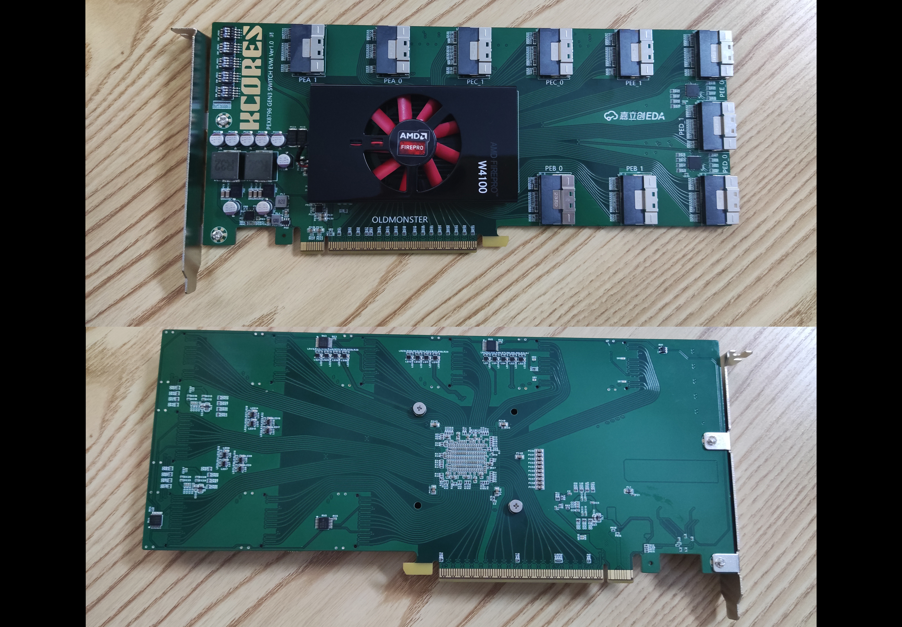
Physical Display


Design Considerations
This card is JLC3313 laminated with 6 layers, and the differential line impedance is 85OHM. The minimum is 6 layers, and 4 layers cannot be designed.
The core 0.9V power supply current of PEX8796 is very large, which is the main power consumption of this card. It is recommended to design with a peak value of 0.9V 35A or above. This card must be equipped with a radiator, and the radiator must be active, because the power consumption of PLX will follow the chip. The temperature rises linearly, and the operating temperature allowed by PEX8796 is very high (it can operate normally if it does not exceed 125 degrees). At this time, the power consumption will be three times higher than the normal power consumption. Therefore, heat dissipation and power supply must be done well.
Other
Demo:

The three-card matryoshka pattern of group friends (three cards in series):
Demonstration of three matryoshka dolls by group friends
Supporting test daughter card:
SlimSASCEMx8_EVM - JLC EDA open source hardware platform (oshwhub.com) (JLC3313 four layers)
Matching PCIE baffle:
LSI server SAS RAID array card PCI-E standard 4U half-height full-height heat sink 2U baffle-Taobao (taobao.com) (select full height)
Matching radiator:
Lenovo R5 340 half-height graphics card radiator fan FS1240-A2042A-Taobao (taobao.com) (Choose 12V, this fan is a bit noisy, if you dislike the noise, you can connect the red wire to the 5V inductor)
Designed by KCORES_OldMonster (from OSHWHub)
Link:https://oshwhub.com/malong/PEX8796_PCIE_GEN3_24PORT_Switch
Design Drawing
Intellectual Property Statement & Reproduction Instructions
This is an open-source hardware project. All intellectual property rights belong to the creator. The project is shared on the platform for learning, communication, and research only; any commercial use is prohibited. If your intellectual property rights are infringed on EasyEDA, please notify us by submitting relevant materials in accordance with the Rules for Complaints and Appeals of IPR Infringement.
Users must independently verify the circuit design and suitability when replicating this project. All risks and consequences are borne by the user, and the platform assumes no liability.
 Empty
Empty
Comment