

 Completed
5.8Ghz diagram of aircraft design
PRO 5.8Ghz diagram of aircraft design
License
:Public Domain
Description
B station collection (can only be opened on the computer):
Function verification video link:
Power detection video link:
Open source is not easy. I hope everyone will support and like it. Collect and follow, and you won’t get lost if you follow it.
QQ group: 595223820.
The platform of LC can upload up to 50M files. If the file is too large, it cannot be uploaded. The original file will be uploaded to the QQ group.
If you have any questions, please feel free to discuss them.
Basic introduction to engineering
This project is mainly to design the 5.8Ghz image transmission of the aircraft and realize the transmission of video signals from the camera on the aircraft.
This project mainly includes schematic design, PCB design and circuit simulation. Schematic and PCB design account for up to 30% of this engineering workload, and circuit simulation is a very time-consuming and cumbersome process.
Why perform circuit simulation?
5.8Ghz is a high-frequency circuit, in order to effectively transmit the video signal of the camera on the aircraft. Impedance matching is required. As for impedance matching, this project provides a feasible method for simulation.
To do simulation, you must first complete the schematic design, select the impedance matching capacitor and inductor components, confirm the stacked structure, and preliminary design of the PCB, and then perform circuit simulation on the preliminary PCB design.
The stacked structure determines the stacked structure set during simulation. This is very important! ! !
This circuit board is 4 layers, and the stacked structure is 7628! ! ! ! ! ! (Changes in the stacked structure will affect the impedance)

Based on my experience in doing this project, the following design process is given. This process is ideal. Suppose you want to replace the components, capacitors and inductors required for impedance matching, and everything starts again...
(So the simulation of high-frequency circuits is very time-consuming and cumbersome)

This project provides detailed simulation steps, see the specific design section.
The basic circuit or interface is shown in the figure below, which mainly includes power circuit, radio frequency + PA circuit. The power interface supports 3S and 4S batteries. VIDEO is the video input interface; PDET is the PA output power detection interface.

You can short-circuit the parts as shown in the figure for frequency selection and select the signal transmission frequency to be used.

The signal transmission frequency that can be selected by shorting is shown in the figure below.

An interface for SPI programming is also reserved for frequency selection.

Through SPI programming, the signal transmission frequency that can be selected is shown in the figure below.

The PA chip RFPA5542 has a 3-level amplification circuit. You can short-circuit the part shown in the figure below and choose to use a 1-level, 2-level or 3-level amplification circuit.

This circuit board is 4 layers, and the stacked structure is 7628! ! ! ! ! ! (Changes in the stacked structure will affect the impedance)
This stacked structure also determines the stacked structure set during simulation.

Simulation results for two transmission lines:
S parameters:


VSWR

Electromagnetic field at the top

Physical Test:
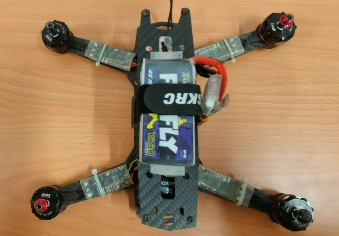
5.8G image transmission installation diagram.

Circuit board front.

Reverse side of circuit board.

Overall picture

Function verification picture:

Power detection picture:
Use an RF power meter and connect an external 30db signal attenuator.


Using two-stage amplification and an external 30db attenuator, the signal power is:
-13+30=17dbm=50mW
-10+30=20dbm=100mw
Using two-stage amplification, the signal transmission power is between 50~100mw.


Using third-order amplification and an external 30db attenuator, the signal power is:
-2+30=28dbm=640mW
-3dbm+30=27dbm=500mW
Using two-stage amplification, the signal transmission power is between 500~640mw.

B station collection (can only be opened on the computer):
Function verification video link:
Power detection video link:
An aside, the ESCs and flight controllers made for the previous LC Competition were on this quadcopter.
ESC:https://diy.szlcsc.com/p/CLZ1/ji-yublheli-diesc
Flight control:https://diy.szlcsc.com/p/CLZ1/f405-fei-kong
Specific design part
Aircraft Design 5.8Ghz Image Transmission Catalog
1.5.8Ghz image transmission 11
2. Principle: Amplifier working status, paranoid network and impedance matching 11
3. Schematic and PCB design 14
4. PCB simulation: HFSS 3D Layout 16
4.2 PCB1 simulation results 41
4.3 PCB1_1 simulation results 45
4.4 PCB1_2 simulation results 48
4.5 PCB1_1 has better simulation results than PCB1 and PCB1_2. Why is PCB1_1 not used? 49
1. 5.8Ghz image transmission
The image transmission of the aircraft includes two parts: sending and receiving. This project is responsible for the image transmission transmitting part; the main function is to transmit the video signal of the camera on the aircraft.
The chips used in the current mainstream 5.8Ghz image transmission are basically RTC6705. The schematic diagram of RTC6705 can also be found online. However, for a person who is new to high-frequency signals, it is difficult to make a functional one even if there is a schematic diagram. Picture transmission, so many people are discouraged.
I will explain the principles based on my own understanding. If there is something wrong, I hope you can point it out and make progress together.
2. Principle: Amplifier working status, paranoid network and impedance matching
For the principle part, please refer to the working status and paranoid network of the amplifier in Section 8.3 of "Radio Frequency Circuit Design - Theory and Application" for explanation. I will upload the attachment as well for this book.

Mainly look at 8.3.2 Bipolar transistor paranoid network. Refer to the picture below for explanation.

The picture below is the logic diagram in the RTC6705 data sheet.

The RFout in the book is PAOUT1 and PAOUT2 of RTC6705. Comparing the two pictures, we can see that we need to select appropriate RFC (radio frequency choke), C B and R 4 outside PAOUT1.
Mainly introduce RFC (radio frequency choke): RFC is an inductor. We all know that inductor passes DC and blocks AC. In this circuit, the function of the inductor is fully demonstrated. After passing from VCC (DC voltage) through R 4 and RFC, the transistor is given the appropriate voltage and current. For the high-frequency signal (AC) coming out of RFout, RFC is equivalent to a circuit break.
The high-frequency model of the inductor is shown in the figure below. At a certain frequency, the inductor will self-resonate, and its self-resonant frequency is called SRF.

Among choke applications, SRF blocks the frequency of the signal most effectively. At frequencies below SRF, impedance increases with frequency. At SRF, the impedance reaches its maximum value. At frequencies above SRF, impedance decreases with decreasing frequency. As shown below.

Therefore, in an ideal state, an inductor with a self-resonant frequency slightly greater than the highest frequency of the signal should be selected. In this ideal state, an inductor with a self-resonant frequency of 6Ghz can be selected.
C B DC blocking capacitor passes AC and blocks tributary current, and directly connects the AC signal that is not blocked by the RF choke to the ground. C B 20pF, R 4 10ohm. (The selected sizes of C B and R 4 are not the point. What is important is the selection of the RF choke and making the impedance of the transmission line 50ohm)
You can also use 10pf, 0ohm to understand its role in the circuit, which is the most important thing.
The most important thing for impedance matching is to know the output impedance of the signal source.
The picture below shows the RTC6705, the original words on the data sheet. Before filtering, there is proper matching at the PA output. The output impedance should be 50ohm.

The input and output impedances of the RFPA5542 PA are both 50ohm.
So we need to make the impedance of the transmission line 50ohm , that is, the two transmission lines shown in the figure below.

This requires the use of HFSS 3D Layout for simulation.
3. Schematic diagram and PCB design
See the blueprint section.

Announcements:

The transmission line width should remain constant so that the pad width and transmission line width are consistent. This makes impedance matching easier.
The width of the transmission line in this project is 0.3mm.

The impedance is about 56ohm.
4. PCB simulation: HFSS 3D Layout
First of all, HFSS 3D Layout simulation requires files in ODB++ format or other formats (I use ODB++ format files). Easy EDA cannot export them directly, so you can only use Easy EDA to export files in Altium Designer format first. , and then use Altium Designer to export files in ODB++ format.
The detailed simulation steps of PCB1 and the simulation results of PCB1_1 and PCB1_2 are given.
4.1 PCB1 simulation steps
1. Export PCB files in LC EDA into Altium Designer format files;

2. Unzip the exported file and open it with Altium Designer;

3. After importing, it was found that the copper coating was not possible, and the two middle copper layers were not possible either; add the middle two copper layers, re-copper coating, and define the layout. After processing, as shown in the figure below.

4. Export files in ODB++ format, as follows;

5. Only the top, bottom, middle two layers and mechanical layer 1 need to be exported; only the saving operation is left and will not be displayed again.

6. Open Ansys Electronics Desktop and import files in ODB++ format;

7. Import the PCB1.tgz file generated when generating the ODB++ format file, and click OK.

8. Then click OK.

9. After importing, it will look like the picture below. Click Save to save.

10. Click here to set the display format;

11. Set according to your own preferences, I like to set it to Display Solid;

12. After the setting is completed, the effect is as shown in the figure below;

13. Click here to set the stacked structure;

14. Set up the laminated structure of JLC. The laminated structure of JLC is as follows;

15. Set thickness to the thickness of the JLC stack, and set each layer to display (that is, the front column, put a check mark);

16. After the settings are completed, click Apply and Close; the effect is as shown in the figure below;


17. Click HFSS Extents and Edit in sequence, as shown in the figure;

18.Set Horizontal and Positive to 30mm; click OK.

19. Click HFSS Extents and Show in sequence, as shown in the figure;

20. Reduce the page appropriately and adjust the appropriate position, as shown in the picture; the squares, these are the two 30mm just set; use HFSS 3D Layout simulation, it must be carried out in a limited space, and the limited space set is as shown below shown in the square.

21. Click HFSS Extents and Hide in turn, as shown in the figure; hide the limited space set (it is just invisible, but it still exists, it is okay not to hide it, I personally like to hide it)

22. Click Orient and Fit All in sequence; after clicking, the effect is as shown in the picture, that is, the circuit board is squared and easy to operate.

23. Click View, Components;
24. The components and chips on the circuit board will be displayed on the right;

25. Click IC, RTC in turn; right-click on RTC, Create Ports On Component;

26. Select $1N154240 on the pop-up page;
27. Click EM Design;

28. Set HFSS Type to Gap; as can be seen from the figure below, the default Port is 50ohm;

29. Repeat steps 25-28, and set $1N59286, $1N154747, and $1N103981 as Ports. The locations are as follows;

30. The picture below is a side screenshot of the completed setting;

31. Select the 6.8nH inductor and click Model Info;

32. Select Library;

33. Click Library Browser;

34. Find the selected inductor model (LQW15AN6N8G00D) on the pop-up page, and its self-resonant frequency is about 11Ghz. The self-resonant frequency 6Ghz given below on the LCSC is the Self Resonant Frequency (GHz min.) in the data sheet. Click Apply, click OK;
(I thought that the self-resonant frequency 6Ghz given below on the LCSC was its self-resonant frequency. It was actually Self Resonant Frequency (GHz min.); when I was screening components, I directly searched for 6Ghz and chose it. Simulation I didn’t pay attention to it at the time, but later I found that the self-resonant frequency was about 11Gh, but the simulation results were okay, so I continued to use it. The self-resonant frequency of PCB1_1 was selected to be 6Ghz, but that component was not in stock) ;


35. Also set the two 10pF capacitors to the selected models; click Apply and OK;


36. Click in sequence, as shown in the picture;

37. Set the frequency to 5.8G on the pop-up page and click Confirm;
38. Set the sweep frequency to 5.3-6.3Ghz and click to confirm;

39. Click HFSS 3D Layout, Validation Check in sequence;

40. If the display shows no errors, there is basically no problem with the simulation settings;

41. Click Setup1, right-click, and click Analyze to start simulation;

42. In the Progress bar of the status bar below, you can see the simulation progress; just wait for the simulation to complete;

43. When the frequency sweep is displayed, the simulation ends and the results can be viewed;

44. What is simulated is the loss, impedance and standing wave ratio of these two transmission lines;

4.2 PCB1 simulation results
45. Right-click on Results and the steps are as follows;

46. Select on the pop-up page
dB(S(RF1.1.$1N103981,U1.13.$1N154747));
dB(S(U1.13.$1N154747,U1.13.$1N154747));
dB(S(U1.3.$1N59286,U3.35.$1N154240));
dB(S(U3.35.$1N154240,U3.35.$1N154240));and click New Report;

47. The simulation results are shown in the figure below;
As can be seen from the figure, at 5.7-5.9Ghz, the two lines S11 are both less than -25dB; at 5.7-5.9Ghz, S21 is basically 0. (The two lines of S21 overlap)

48. Right-click on Results and the steps are as follows;
49. Select on the pop-up page
S(U1.13.$1N154747,U1.13.$1N154747); S(U3.35.$1N154240,U3.35.$1N154240);And click New Report;

50. The simulation results are shown in the figure below;
It can be seen from the figure that at 5.8Ghz, the real parts of the impedances of the two transmission lines are above 45ohm and below 55ohm.

51. Right-click on Results and the steps are as follows;

52. Select VSWR on the pop-up page;
VSWR(U1.13.$1N154747); VSWR(U3.35.$1N154240); And click New Report;

53. The simulation results are shown in the figure below;
It can be seen from the figure that at 5.7-5.9Ghz, the standing wave ratios of the two transmission lines are less than 1.11.

4.3 PCB1_1 simulation results
1. The simulation is the loss, impedance and standing wave ratio of these two transmission lines;

2. The 6.8nH inductance is selected as LQG15WZ6N8J02(LQW15AN6N8G00D, that is, 6.8NH inductance in PCB1, is not available in stock at present), and the self-resonant frequency is about 6Ghz. The inductance and capacitance on the rest of the transmission line are the ideal inductance and capacitance.

3. The simulation results are shown in the figure below:
As can be seen from the figure, at 5.7-5.9Ghz, the two lines of S11 are both less than -36dB; at 5.7-5.9Ghz, S21 is basically 0. (The two lines of S21 overlap)

4. The simulation results are shown in the figure below:
As can be seen from the figure, at 5.8Ghz, the real parts of the impedances of the two transmission lines are both around 50ohm.
5. The simulation results are shown in the figure below;
It can be seen from the figure that at 5.7-5.9Ghz, the standing wave ratios of the two transmission lines are less than 1.04.

4.4 PCB1_2 simulation results
Animate_log graph
4.5 PCB1_1 has better simulation results than PCB1 and PCB1_2. Why is PCB1_1 not used?
Because:
A. The 6.8nH inductor (LQG15WZ6N8J02) is out of stock. It is in stock and can be made again;
B. In the simulation of PCB1_1, the inductors and capacitors on the two transmission lines are ideal components. They do not use components from a specific component library like PCB1 and PCB1_2. There must be a deviation between the simulation results and the actual ones. I don’t know if they will be better than the actual ones. It's still bad. If it's worse than the actual one, it's not directly G;
C. Selecting components and running the simulation is a very tedious process. Currently, the simulation files, whether good or bad, are tens of gigabytes in size. The simulation can really run all day and night.
D. Provide an idea to friends who like and are interested, so you can try it yourself.
5. Physical Test
5.8G image transmission installation diagram.
Circuit board front
Reverse side of circuit board
Overall picture
Function verification picture:
Power detection picture:
Use an RF power meter and connect an external 30db signal attenuator.
Using two-stage amplification and an external 30db attenuator, the signal power is:
-13+30=17dbm=50mW
-10+30=20dbm=100mw
Using two-stage amplification, the signal transmission power is between 50~100mw.
Using third-order amplification and an external 30db attenuator, the signal power is:
-2+30=28dbm=640mW
-3dbm+30=27dbm=500mW
Using two-stage amplification, the signal transmission power is between 500~640mw.
B station collection (can only be opened on the computer):
Function verification video link:
Power detection video link:
An aside, the ESCs and flight controllers made for the previous LC Competition were on this quadcopter.
ESC:https://diy.szlcsc.com/p/CLZ1/ji-yublheli-diesc
Flight control:https://diy.szlcsc.com/p/CLZ1/f405-fei-kong
6.Remarks
1. "Radio Frequency Circuit Design - Theory and Application" This book is too big at 116M and cannot be uploaded. The maximum upload is 50M. Only the working status of the amplifier and paranoid network in Section 8.3 are uploaded.


2. The original file of HFSS 3D LAYOUT simulation is more than 600 MB, and it is still more than 400 MB after compression, so there is no way to upload it directly and give the network disk link.
Link: https://pan.baidu.com/s/1fEJYfRwdB43qmpmRgGhqow
PWD:30hl

3. Personal contact information QQ: 2995001663 QQ group: 595223820.
This platform can upload up to 50M files. Files that are too large cannot be uploaded. The original files will be uploaded to the QQ group.
If you have any questions, please feel free to discuss them.
4.Hope everyone will support me, like, comment and collect.
Designed by DroneCYF (from OSHWHub)
Design Drawing
 Empty
Empty
Comment