


© 2024 EasyEDA Some rights reserved ISO/IEC
Editor Version
×
Standard

1.Easy to use and quick to get started
2.The process supports design scales of 300 devices or 1000 pads
3.Supports simple circuit simulation
4.For students, teachers, creators
Profession

1.Brand new interactions and interfaces
2.Smooth support for design sizes of over 5,000 devices or 10,000 pads
3.More rigorous design constraints, more standardized processes
4.For enterprises, more professional users

Ongoing
STD How are Printed Circuit Boards (PCBs) recycled?
License: CERN Open Hardware License
Mode: Editors' pick
- 0
Update time:
2019-03-04 07:37:53
Creation time:
2018-12-04 06:34:33
Description
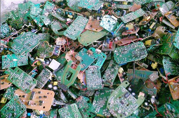
Waste PCB has a variety of recyclable precious metals, such as tin, copper (high in circuit), gold, silver, nickel, palladium, and other non-metallic materials.
[](
Metal materials): Circuit board recovery equipment (A type of high voltage electrostatic separation);
[]( Non-metallic materials): Non-metallic materials of circuit boards;
Thus, the comprehensive handling and recycling of waste circuit board has become an important subject in the field of resources and environment.
Design Drawing
schematic diagram
(
1
/
)
PCB
(
1
/
)
The preview image was not generated, please save it again in the
editor.
BOM
Project Members


 0
0
 0
0
Collect to album
Target complaint
Related Projects
Change a batch
Loading...
Add to album
×
Loading...
reminder
×
Do you need to add this project to the album?