

PCBThrough-hole pins not connecting to power plan
2025-10-13 20:29:55
0
1
0
So this is a common problem people have, tons of posts about not getting connections to internal power or ground planes. I have done a dozen 4-layer designs in Easyeda and (thought) I understood how it works, but on my latest design... I cannot get the through-hole pins on the power net to get automaticallyl connected to the internal power plan (they remain as ratlines to be manually routed). So here I think are all the relevent bits that taken together, I thought, should work (netflag on power net, net name matches PCB layer name, PCB layer is "Plane" type, board outline has no gaps, PCB planes have been rebuilt, the power plane covers all area inside the board outline.
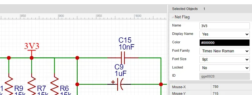
Schematic: Power net is named "3V3" and has a netflag named "3V3". Notice + side of C9 is connected to net "3V3".
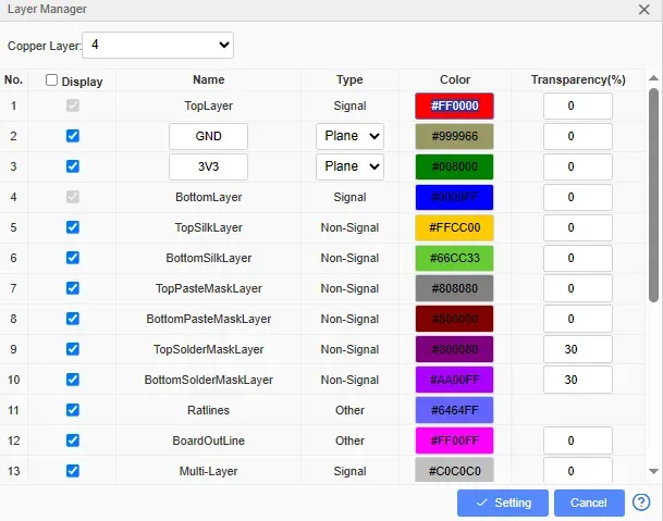
PCB Layer Manager:
Here is that C9 component. Just did Shift-B to make sure all copper is rebuilt.
With the 3V3 layer selected you can see the + terminal is isolated from the 3V3 plane, but the netname on that ratline is 3V3. So why is that + pin not connected to the 3V3 plane?
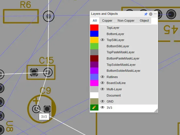
C9 is just one example, every place a pin should connect to the 3V3 plane, it does not.
What else is there? I am stumped!
Popular Posts
More
Comment