

 Ongoing
Class D Amp Workshop
STDClass D Amp Workshop
License
:Public Domain
Description
Before You Continue:
I made a schematic version for this project in Class D Amp - OSHWLab
I intended to merge the two projects together, but I don't think EasyEDA allows me to that very easily. The PCBs from this project should match up with the schematics in the other project. So, I will use this project page for the PCB kit and assembly only. The other project will have all of the schematics and theory. The only PCB missing from this page is the SOIC to 8-DIP adapter, which is in the other project. Please also refer to the detailed BOM in the attachments. Do note that the BOM is set for 30 kits by default... please adjust this number accordingly.
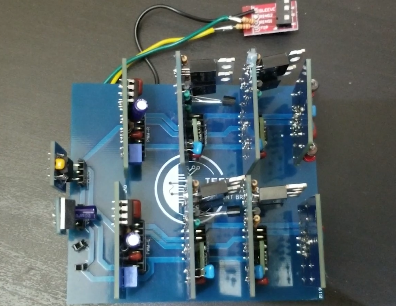
PCB Modules:
The three different schematics for a Class D Amplifer (Mono Half-Bridge, Stereo Half-Bridge, and Stereo Full-Bridge) correspond to the modules of the PCB kit. Thus, the "motherboard" supports all three types naturally and can be exapnded accordingly to Stereo Full-Bridge. The reason for this design is because although it seems unconventional to use male-female header pairs as modules with the high frequency circuitry, PCB kit is meant as a teaching tool for students to learn how each block in the Class D Amplifer work together to amplify audio. This way the students can continue to expand their kit and max out their modules as they continue to reach each milestone.
Assembly Process (Abridged):
-
Please use a 12V power supply limited at 150mA and an oscilloscope to view and test out the modules. You may also choose to have female SIPS installed in your motherboard to make things hot-swappable. The scope this project do not include a power supply, oscilloscope, AUX cable, or speakers in the materials list.
- Focus on building one audio channel at a time. Repeat all steps when starting the other audio channel. Please cross-reference every component in your inventory with the Designator in the attached BOM and the labels on the PCB silkscreen.
-
Solder the Audio jack, 12 V power line, and GND power line.
- Solder the Voltage Regulator PCB (VReg)
-
On the oscilloscope, the module should have an expected output of a nice 5VDC on the +5V pin.

-
-
Solder the Clock PCB
-
On the oscilloscope, the Clock module's output should have a sawtooth waveform of around 270 - 300 KHz on the TRI pin (See Channel 1 [Yellow] in Fig 1). Keep this probe on.

-
-
Solder the PWM Modulator PCB
-
The PWM Modulator module has a potentiometer that adjusts the added DC offset to your audio signal. Use a second probe to test the offset voltage by hooking it onto the positive terminal of C3. The footprint of C3 should be relatively large, so use that to your advantage. Make sure the oscilloscope is not adding any offset to the signals and their no load signals are perfectly on the x-axis. Also, please check that the voltage per division of each channel is the same. Once you have made these checks, adjust the potentiometer such that offset voltage is perfectly in the middle of of the sawtooth waveform amplitude (See Channel 2 [Blue] in Fig 1).
-
Another way to check is to have a probe on the SQ+ pin and another on the SQ- pin, with both probes on 10x attenuation. Then, adjust the potentiometer so you have about 50% duty cycle for both signals.

-
-
Solder the Full/Half Bridge Driver PCB
-
On the oscilloscope, the Full/Half Bridge Driver should have an amplified SQ+ signal on the SQ++ pin. Please note that using 1x attenuation may add parasitic capacitances that could be lethal to the MOSFET driver when under load. Always use 10x attenuation when probing SQ++/SQ-- pins!
-
If doing Half-Bridge, solder one Full/Half Bridge Driver module. If doing Full-Bridge, solder two Full/Half Bridge Driver modules. You only need to oscilloscope check one of them.

-
-
Solder the Filter PCB
-
Follow the Filter Schematic in this project page carefully to understand what you're doing
-
If Half-Bridge, add C16, Do not add C13-15 - shorting out their terminals. Do not add L3 and L4 either.
-
If Full-Bridge, remove C16 - shorting out their terminals add remaining components as intended.
-
Solder a 4 Ohm speaker to the output of the Filter

-
-
Connect the audio jack to your device. Do not play audio yet and keep volume at 0% for now. With everything powered on:
-
Do the calibration in Step 6 again. This is because the speaker load feedback noise into the low voltage inputs.
-
You will notice that when you adjust the potentiometer, the current reading on the power supply changes too. The current reading should be minimum if the calibration is done correctly, resulting in highest efficiency.
-
-
Play some music


Fig 1: One of the methods for the calibration step.
Special thanks to McMaster University and Voltera for making this possible! I would not be able to get the required components and lab resources without my university. I would also not be able to prototype PCBs without the Voltera V-One PCB Printer. It's very convinient that I can prototype PCBs now without having to wait 1-2 weeks from JLCPCB for every PCB iteration. I'd also like to thank Abin Raju from Datec Coating Corporation for connecting me with Voltera.
Design Drawing
BOM
 Clone
CloneProject Members
 Empty
Empty
Comment