

 Ongoing
Gooser5
STDGooser5
License
:Public Domain
Description
After running out of ideas to try and make Gooser4 work (update: it ended up working after all), I decided to rework Gooser3 for standard 3.3mm mosfets. I intended to keep the changes minimal just to test if it would work, but it took on a life of its own and I ended up with a lovely single-sided design (aside from the usual back-side capacitors and optional heavy copper bars). I like it better than Gooser4 for all but the most size-critical applications, and I've refined it even further since the initial release.
https://community.simplefoc.com/t/gooser-a-4-in-1-lepton-derivative/5325/95
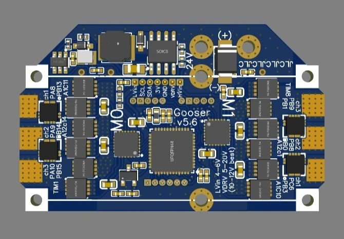
The primary design is for 2 motors, and can be tiled for more, or trimmed smaller for one motor. The 0402 capacitors below the CPU are the southernmost essential components. Minimum board size is 21x32mm, or 21x31mm with a few edits.
Typically, programming is done using an STlink and debugging done with Arduino serial monitor via an FTDI adapter, both of which connect to the 6-pin programming connector.
There are four power rails on the board:
HV_IN: Power to mosfets. No minimum voltage, max depends on rating of mosfets, capacitors, TVS diode, buck converters.
VDRV: Power to gate drivers. 20V max, minimum depends on mosfet Vgs (most need 10V for full on).
LV_IN: Power to 3.3V regulator. 4V minimum, maximum limited by 500mW waste heat. Around 9V depending on encoder power use, or ~12V on single-motor boards. CPU uses ~35mA but can be reduced by lowering clock rate, current sensors use 5mA each, hall sensors usually 5mA each, encoders usually around 15mA.
3V: Power to MCU, current sensors and encoder connectors. Typically 3.3V, though anything 3-3.6V is within spec.
There are optional buck converters outside the tileable area to supply power to LV_IN and VDRV. If the bucks are not populated, LV_IN and VDRV must be supplied externally. VDRV can be connected to HV_IN if it is below 20V, or the third cell of a lipo battery via the balance connector. LV_IN can be powered from the first cell of a lipo, or connected to VDRV if power usage is low enough (e.g. single motor, or dual motor without encoders). It's also possible to leave LV_IN unpowered and directly supply 3V, bypassing the onboard regulator.
CAUTION! If low voltage buck is populated, you must not supply external power to LV_IN or connect LV_IN to VDRV. If high-voltage buck is populated, you must not supply external power to VDRV or connect VDRV to HV_IN. However it is safe to use LVin and/or VDRV as power outputs in this case. The buck converters have plenty of current to spare.
The encoder connectors have 5 pins each: 3V, GND, and 3 ADC pins. This allows using two linear halls spaced 90 degrees, or 3 linear halls spaced 120 degrees to give potentially better accuracy, and redundancy if one fails. Also can use 3 digital halls, though they usually need more than 3.3V. The encoder connector 3V pins can be isolated from the rest of the 3V rail by disconnecting the exposed trace next to the M0 encoder 3V pin. The 3V hole on the aux connector goes with them, so it can then be used as power input to the encoder pins.
There is a complete set of SPI pins among the two encoder connectors, so SPI encoders can be used. Also I2C encoders via the aux pin header. There are two TIM2 pins on M0's encoder and two TIM3 pins on M1's, so I think hardware counting of ABZ encoders will work too.
This board is designed primarily for SMD electrolytic capacitors (8x8mm or 10x10mm), though you can still use ceramics and through-hole electrolytics like previous versions. The connectors fit between them when soldered on the back side, which leaves the front side clear so it can be stuck to a heatsink. There are three good arrangements for SMD electrolytics, which give 660uF per motor with 50V capacitors. Not quite the 1000uF Valentine recommended on Lepton, but hopefully enough.
* Three 8x8mm per motor for single and dual motor boards.
* Two 10x10mm per motor for single motor with buck converters.
* Two 10x10mm plus three 8x8mm per pair of motors for quad motor boards.
Two 10x10mm per motor can be used in other cases with some caveats. There are two positioning options: centered, and shifted toward the power input/buck converter area.
* Centered is good on any board variant, but one of the capacitor solder pads goes under the encoder connector, preventing it from fully seating to the board. You can use a 4-pin connector if you don't need access to the outermost pin, or solder wires directly to the board, or put the connector on the other side.
* Shifted is fine for the top row on quad motor boards, but on the bottom row it partially obstructs the lower positive power input hole (not a problem if you plan to use the upper positive hole beside the negative hole).
Other design notes:
* Bus voltage sense ADC max corresponds to 39.1V bus.
* The timer channels and motor phase names don't match the DRV8300's pin names in the schematic, but from a programming perspective timer channel 1 controls phase A and so on.
* The current sensors' capacitors on the back are 0603 size for easier hand soldering.
* It is possible to solder an XT30 connector (LCSC part C428721) to the power input holes if you rotate the M1 encoder connector 180 degrees so it doesn't collide.
* The programming connector can't be properly mounted on the top side of the board. It will work, but will be crooked, tipped up over the edge of the CPU. This was a sacrifice made to fit the larger 3V regulator. Usually the connectors are mounted on the back side with the capacitors anyway.
Notes on each variant of the board:
Gooser5.7-dual: The basic two motor version with bucks.
Gooser5.7-quad: Four motor version. Adds one copy of the tileable area, and extra input area on the left which enables stacking two boards face-to-face and the input terminals line up.
Gooser5.7-single: Basic single-motor version with buck converters. Low-voltage buck is typically not needed, so its components can be left unpopulated and join LV_IN to VDRV instead. The capacitors below the CPU have been moved a bit to allow trimming to 21x31mm size, and an extra hole for PA4 since it gets removed in that case.
Gooser5.7-minimal: Single-motor that's already been trimmed to 21x31mm size. No buck converters, so LV_IN and VDRV must be supplied separately, or joined to HV_IN if it's below ~12V. If running below ~14V, this version can use fourteen 22uF 25V 0805 ceramic capacitors and one 470uF or larger electrolytic sticking off the side with the power input wires, or possibly twelve 47uF 25V 1206 ceramics with no electrolytics at all (564uF total).
Quick reference for CPU pin assignments:
Motor 0:
TIM1 ch1 PA8, ch1n PB13, ch2 PA9, ch2n PB14, ch3 PA10, ch3n PB15
Current sense PB12/ADC1ch11, PB11/ADC12ch14
Encoder PA7/ADC2ch4/TIM3ch2, PA2/ADC1ch3/TIM2ch3, PA5/ADC2ch13/TIM2ch1
Motor 1:
TIM8 ch1 PC6, ch1n PB3, ch2 PB8, ch2n PB0, ch3 PB9, ch3n PB1
Current sense PF0/ADC1ch10, PA0/ADC12ch1
Encoder PA6/ADC2ch3/TIM3ch1, PA1/ADC12ch2/TIM2ch2, PA4/ADC2ch17/TIM3ch2
SWD: io PA13, clk PA14
UART3: tx PC10, rx PC11
I2C1: sda PB7, scl PA15
SPI1 (two pins from each encoder connector): nss PA4, sck PA5, miso PA6, mosi PA7
Bus voltage sense: PC4/ADC2ch5
Design Drawing
BOM
 Clone
CloneProject Members
 Empty
Empty
Comment