

 Completed
Bond_Light
STDBond_Light
License
:MIT License
Description
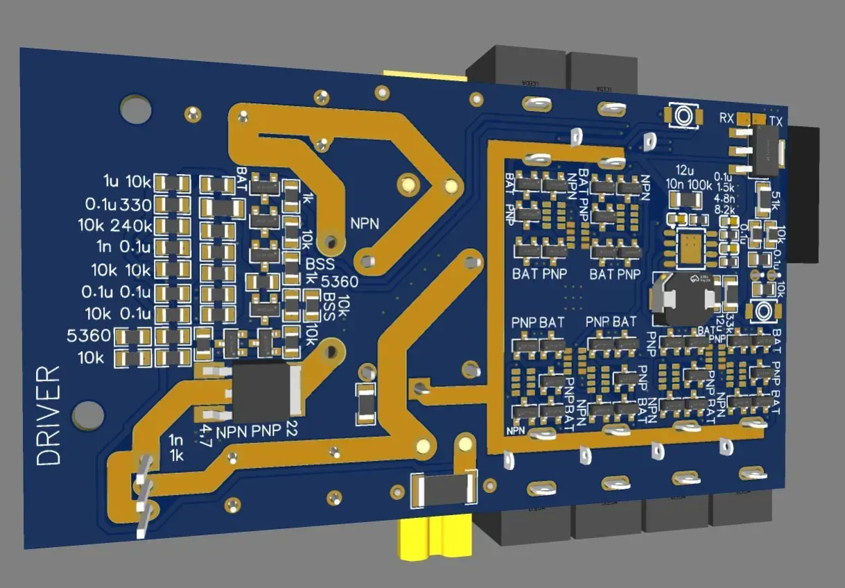
The project began as a simple and reliable prototype: a single-layer board was assembled manually on the basis of ESP32 with an optocoupler driver on PC817C — a solution that provided galvanic isolation between the power section and the microcontroller, protected the MCU from impulse interference and possible overvoltages, facilitated debugging, and increased safety when working with 12 V circuits. A built-in web interface was implemented for the user, allowing them to conveniently configure timers and scenarios and control channels directly from a browser. During testing, important limitations of the initial architecture were revealed: the optocoupler did not provide stable operation above ≈5 kHz, and the MOSFET gate discharge through a passive resistor was too slow — this complicated the use of high-frequency PWM and led to flickering and unclear control at low brightness levels. Therefore, the project underwent a major upgrade: a two-layer printed circuit board was developed and manufactured at the factory, the component base was optimized to minimize cost without compromising reliability, power supply and protection were improved, and a full-fledged software and network infrastructure was implemented — a native Android app for convenient local control, a fast and responsive interface via WebSocket/HTTP, and the ability to access it remotely via an MQTT broker, making the device compatible with smart home ecosystems. The key hardware innovation is a proprietary gate driver based on simple bipolar transistors in a push-pull circuit, which provides sharp edges and signal decay at a PWM frequency of ~30 kHz. This allowed us to implement 10-bit PWM and achieve truly smooth, detailed brightness control from 0 to 100% (eliminating the problem of “insensitive” 1-4% levels). Additionally, a built-in battery charging system with the ability to program the charging current and a power source relay switch for seamless transition between mains and battery power have been integrated, making the device practical and ready for commercial use. The project was accompanied by engineering tests (PWM verification, gate rise/fall measurements, thermal control, EMI and stability testing under sustained loads) and documentation: schematics, Gerber/BOM, test reports, photos, and demo videos. As a result, this is not just a working prototype, but a product concept with a mature hardware platform, optimized BOM, convenient UX, and a control network.
Design Drawing
BOM
 Clone
CloneProject Members
 Empty
Empty
Comment