

 Completed
Schematic Diagram And PCB ( AKMAL AQIL )
STDSchematic Diagram And PCB ( AKMAL AQIL )
License
:Public Domain
Description
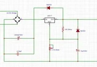
The schematic diagram represents a low-voltage DC power supply based on a 230 V AC mains input. The AC voltage is stepped down by a transformer to about 20 V AC, which is then fed into a full-wave bridge rectifier to convert it into pulsating DC. A large electrolytic capacitor smooths the rectified output before it enters an LM317 adjustable voltage regulator. Supporting resistors connected to the LM317 set the desired regulated output voltage, while diodes such as the 1N4002 provide protection against reverse polarity and back-feeding. Additional capacitors further reduce ripple, ensuring stable output.
The PCB layout corresponds to this schematic, showing proper placement of the transformer, rectifier bridge, capacitors, LM317 regulator, and terminal blocks. Power traces are kept thicker to handle current flow, and the components are arranged logically to match the schematic flow—from AC input to DC output. The layout includes clear labeling for AC inputs, DC outputs, and component polarity, helping ensure correct assembly and reliable operation of the regulated power supply.
Design Drawing
BOM
 Clone
CloneProject Members
 Empty
Empty
Comment