

 Completed
Report Schematic Diagram and PCB
STDReport Schematic Diagram and PCB
License
:Public Domain
Description
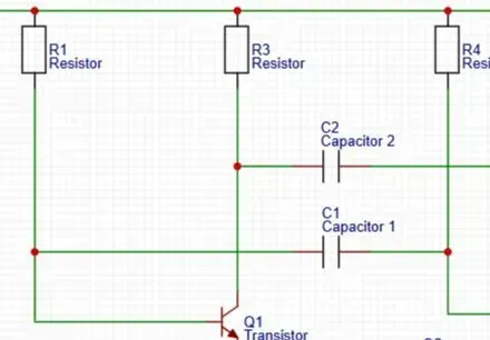
This project features a transistor-based circuit designed for signal switching and timing control, implemented through a clear schematic and corresponding PCB layout. The schematic includes two transistors (Q1 and Q2), which operate as active switching elements, along with four resistors and two capacitors that form the supporting biasing and timing network. The capacitors (C1 and C2) provide coupling or delay functions, while the resistors (R1–R4) set current flow and ensure stable transistor operation. The PCB layout arranges these components efficiently, with organized routing for power, signal lines, and grounding. The connector Y1 serves as the circuit’s input/output interface. The board is designed to maintain short, clean traces, reduce noise, and ensure reliable operation of the switching circuit in practical applications.
Design Drawing
BOM
 Clone
CloneProject Members
 Empty
Empty
Comment