

 Ongoing
Full voltage regulation
STDFull voltage regulation
License
:Public Domain
Description
The idea is to take 7.5V or 15V from a Class II no-FG fully isolated power supply, filter out the ripple as much as possible, then use an adjustable regulator to regulate it to an adjustable voltage of 4-6 V at up to 8 A, or 11-13V at up to 6 A. Slow start-up on the order of a significant fraction of a second is acceptable or even desirable, but startup and shutdown overshoot is to be avoided.
Basic design has been shamelessly stolen from Art of Electronics and EEVblog.
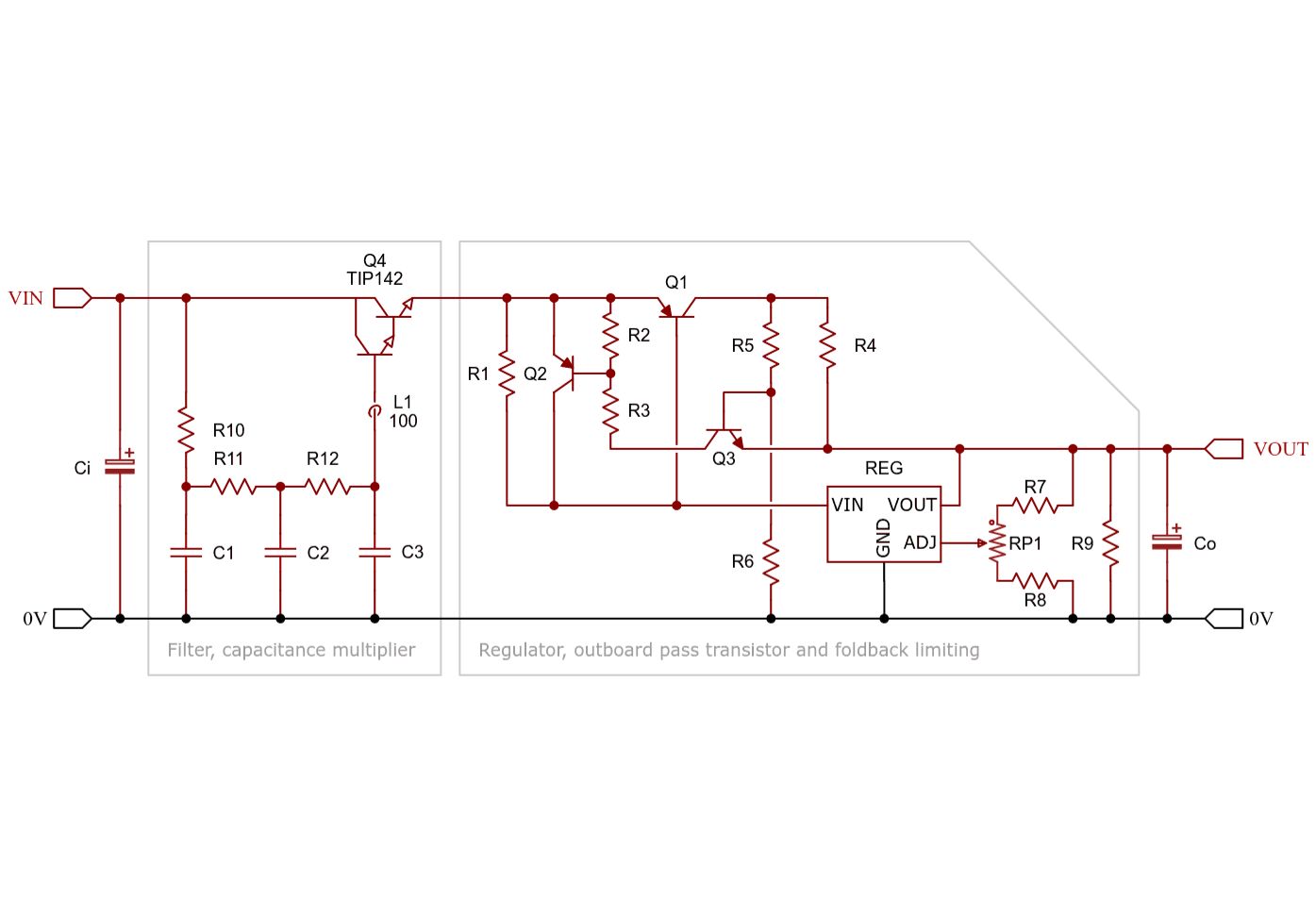
Filter stage – capacitance multiplier
The capacitance multiplier is based on Q4, a TIP142 (or '1 or '0) NPN BJT Darlington transistor. This is to be driven at a base current (Ib) of around 100A or so (50mA to 150mA). (Datasheet quites absolute maximum limit at 500mA, so don't push it.)
L1 is a ferrite bead, 100 Ohm or 120 Ohm suggested. Although the base current should typically be around 100mA and never exceed say 200mA, pick a bead with a high enough current capability and low DC resistance.
R10, C1, R11, C2, R12, C3 forms a three-stage passive low pass filter. A single stage might suffice, two stages should work, and anything beyond three stages is probably overkill. Note that the filter time constant also affects startup time, so it cannot be arbitrarily large.
Given a base current of 50mA, at a 10A collector current TIP142 collector-emitter voltage should be less than 1.5 volts, according to the datasheet. The main selection criteria is high gain, high current carrying capability, and low collector-emitter voltage at high currents. Optimally, at maximum currents, we'd prefer to drop less than a volt here.
Regulator stage
The regulator stage adapts AoE figure 9.109 B. Q1, Q2, Q3, R1 are the same in both. R2-R6 define the current limits. R4 here is Rsc. R2 and R3 are the unnamed current limiting voltage divider in AoE, and R5 and R6 implement foldback limiting.
R7, RP1, R8 form a voltage divider controlling the output voltage. Without RP1, VOUT = Vref × (1 + R7/R8), where Vref is the reference voltage the regulator uses, usually around 1.2 volts or so. If we use RP1 for the total resistance across RP1, then
VOUTmin = Vref × (1 + R7 / (RP1 + R8))
VOUTmax = Vref × (1 + (R7 + RP1) / R8)
R9 is minimum load per the regulator requirements (omitted if none). If the minimum load is IOUTmin, then
R9 = VOUTmin / IOUTmin
and the maximum power it dissipates is VOUTmin × IOUTmin.
R1 determines the minimum load at which the pass transistor Q1 starts boosting the output current. AoE uses 0.6 Ohm.
R2-R6 and Q2 and Q3 implement overload protection. When the voltage drop over R4 (Rsc) is large enough, Q2 turns off Q1. (Since Q2 must dissipate the extra power, it must be able to handle the maximum output current load.) R2 and R3 are small resistors (as in R2+R3 is a low value, so that the base of Q2 is driven at sufficiently high currents (50mA-150mA?) if an overload occurs. Without foldback current limiting, R6 is omitted and R5 shorted; so R5 and R6 form a voltage divider that essentially controls how Q3 reacts to different voltage drops over R4 (Rsc).
Q1 and Q2 are PNP transistors, and Q3 an NPN transistor. Q3 only needs to be able to pass enough current to turn Q2 off. A transistor with a decisive turn-on/turn-off base-emitter voltage (Vbe) works best here, so that below the set current limit, Q3 won't affect Q2. Q2 does not normally conduct, it only drops the input voltage over itself whenever the load is too high. It does, however, be able to handle all of the load current in the worst case. So, PNP transistor that does not leak too much (does not conduct in normal operation), and can handle the maximum current load at maximum input voltage (and turn it to heat) works here.
Q1 is the pass transistor. The current drawn by the regulator causes a voltage drop over R1. This voltage drop is the difference between Q1's base and emitter: Vbe = IIN/R1. If the regulator is a linear voltage regulator (and not say a DC-DC switcher), then IIN=IOUT, and Vbe = IOUT/R. So, we need Q1 to not be saturated (unless output current is already above the maximum somehow), and follow Vbe perhaps not linearly, but at least monotonically. Essentially, we want a low emitter-collector drop (Vce) at highest currents, and its maximum current to be high enough that it doesn't saturate in normal operation (and thus follows the regulator).
I think OnSemi MJW1302A, NJW1302G , ECH8102, D44H8, D44H11 might be suitable.
Design Drawing
BOM
 Clone
CloneProject Members
 Empty
Empty
Comment