

 Ongoing
power bank IP5306
PROpower bank IP5306
License
:Public Domain
Description
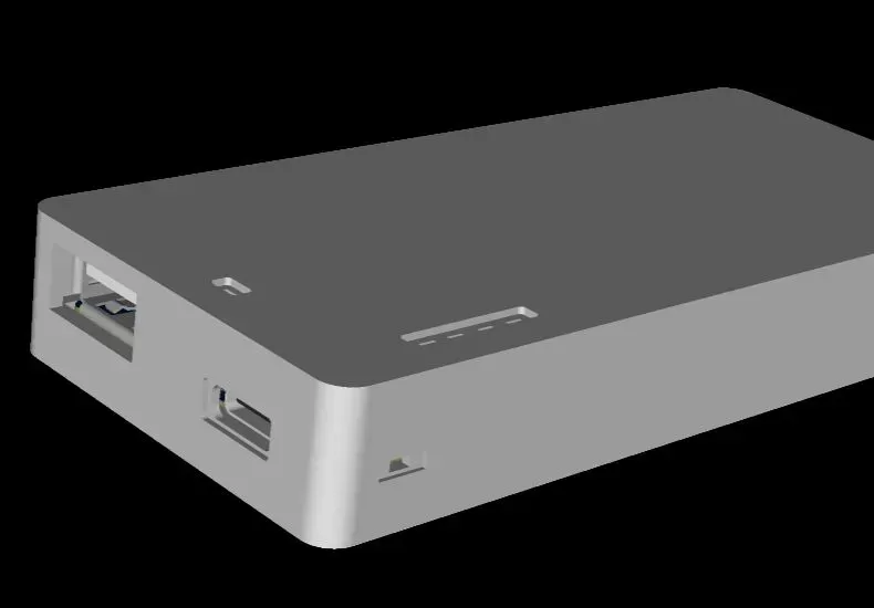
This project is a compact and low-cost USB-C power bank PCB designed using EasyEDA Pro and based on the IP5306 power management IC.
The IP5306 is an all-in-one solution that integrates Li-ion battery charging, 5V boost conversion, power path management, and battery level indication into a single chip, making it ideal for portable power applications.
This design focuses on simplicity, manufacturability, and affordability, making it suitable for beginners, hobbyists, and engineers.
✨ Key Features
-
USB Type-C input for battery charging
-
5V boost output for external devices
-
Single-cell Li-ion battery support
-
Battery level indicator LEDs
-
Push-button power control
-
2-layer PCB for low manufacturing cost
-
All components sourced from LCSC
-
One-click PCB ordering with JLCPCB
🛠 Design Information
-
EDA Tool: EasyEDA Pro
-
PCB Layers: 2
-
Application: Power bank / portable power supply
-
Manufacturing: JLCPCB compatible
📘 Educational Purpose
This open-source project is suitable for:
-
Learning EasyEDA Pro workflow
-
Understanding power management PCB design
-
DIY power bank and portable electronics projects
-
Creating PCB design tutorial content
🌍 Open-Source
All schematic and PCB files are shared openly on OSHWLab.
You are free to study, modify, and reuse this design for learning and personal projects.
🔗 Useful Links
EasyEDA Pro: https://easyeda.com
JLCPCB: https://jlcpcb.com
🏷 Tags
EasyEDA, EasyEDA Pro, IP5306, USB-C, Power Bank, PCB Design, JLCPCB, Open Source
Design Drawing
BOM
 Clone
CloneProject Members
 Empty
Empty
Comment