

 Completed
Design of board-level binocular industrial camera system based on FPGA
PRO Design of board-level binocular industrial camera system based on FPGA
License
:GPL 3.0
Description
1. Requirements analysis
This project aims to design a small and beautiful USB 3.0 binocular industrial camera.
2. hardware design
2.1 Device selection
2.1.1 FPGA selection
This design uses XC7A50T-1FTG256I. Firstly, the package has a small size, large pin spacing, and is convenient for soldering. Its internal logic resources are completely sufficient.
2.1.2 USB Controller Selection
This design uses the FT601Q USB3.0 FIFO chip as the data transmission interface, and the measured loop speed is 350MByte/S.
2.1.3 Image Sensor Selection
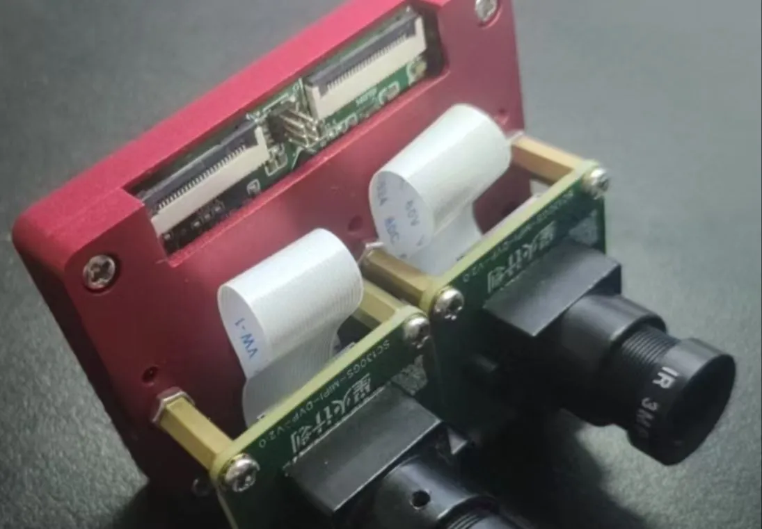
This design uses a black and white SC130GS image sensor with MIPI interface, 1280 * 1024 resolution, 4um pixel size, frame rate 240Hz, and 4laneMIPI interface.
2.1.4 power chip selection
The power chip uses an integrated inductor DCDC TPS82130SILR, which can save some area but increase the welding difficulty. For this type of package, the manual welding method is as follows:
(1) uniformly tin each pad
(2) Apply a layer of flux and place the chip
(3) Hot air gun heating welding
FPC seat welding can also refer to the above process.
2.2 Scheme design
2.2.1 BANK function division
(1) BANK14 and BANK34 contain two sets of USB3.0 buttons, indicator lights, and control signals for the MIPIC MIPID interface, with a fixed voltage of 3.3V.
(2) BANK15 is used to connect DDR3, with a fixed voltage of 1.5V.
(3) BANK35 is used to connect the control signals of four MIPI interfaces and MIPIA MIPIB interfaces, with a fixed voltage of 2.5V.
2.2.2 camera acquisition solution
During the actual use of SC130GS MIPI interface, it was found that MIPI only has HS signal and no LP signal. Therefore, resistance network or level conversion chip (MC20901) was not used in this design. For other models of MIPI interface sensors, if resistance network or MIPI to LVDS level conversion chip is not added, there will be major problems.
For the SC130GS camera board designed this time, the control signals mainly include PWDN, I2C_SCL, I2C_SDA, Trig0. The average voltage is 1.8V, so four four-channel level conversion chips must be added to the FPGA main control board to match the levels at both ends. The MIPIA MIPIB interface uses 2.5V to 1.8V, and the MIPIC MIPID interface uses 3.3V to 1.8V.
2.3 Schematic design
The FPGA main control board schematic mainly includes four parts: FPGA minimum system design (including button LED), DDR3 design, USB3.0 controller design, and camera interface design. Please refer to the engineering schematic for details.
The schematic diagram of the camera mainly includes the peripheral circuit design, interface circuit design, and power circuit design of the image sensor.
In addition, Xilinx downloader and adapter board, FPC to HDMI adapter board are also designed.
3. Software design
3.1 FPGA development
FPGA design mainly includes image acquisition module, camera control module, image caching module, and image transmission module. MIPI acquisition can be done using the open source mipi source code on GitHub or the MIPI netlist in the OVIS XC7A100T board information. The USB3.0 Data Acquisition control uses the FDMA acquisition solution of the MiLianKe FT601Q.
The first time you use USB3.0, you must configure FT601Q to enter 245FIFO mode. Use FT600ChipConfigurationProgUtility this software.
3.2 Upper computer development
This design is based on the upper computer in the FDMA acquisition scheme of the MiLianKe FT601Q for secondary development, adding camera exposure time and gain control functions.
3.3 Welding completion effect
(1) FPGA main control

(2) FPC to HDMI

(3) Version using CNC shell

3.4 System testing
(1) Original image display effect.


For detailed documentation, please refer to the uploaded user manual.
Version description:
V1.0 is the initial version
V1.1 Version Change Record
DDR3_D9 pin changed from H12 to G15
2. DDR3_DM1 pin from G12 to H12
3. DDR3_A4 pin from D9 to D10
4. Leave DDR_VREF pins connected to the external 0.75V, when using the xc7a50tftg256-3 chip, the DDR3 speed can reach 1066MBPS, at this time, external VREF must be selected
5. Add G11 pin as LED output
V1.0 version can achieve arbitrary binocular (2560X1024) image acquisition and arbitrary ternary (3840X1024) image acquisition. When acquiring full frame size quad images, due to insufficient effective bandwidth of DDR3, the image cannot be cached normally
Therefore, in version V1.1, FPGA can choose a -3 level model, and set the DDR3 data rate to 1066MHZ in the MIG IP core to increase the effective bandwidth of DDR3. The four-eye acquisition (2560 * 2048/5120 * 1024) has been verified
V1.2 version change record
1. Remove all camera FPC interfaces and use BTB connectors for more versatility, allowing you to design various daughter card connections according to your needs.
2. All IOs in BANK15 have differential equal length
BTB leads out five levels of 1.5V, 1.8V, 2.5V, 3.3V, and 5V
4. When using single-ended IO, pay attention to its level
Designed by 智工学院杨老师 (from OSHWHub)
Link:https://oshwhub.com/mike0/design-of-board-level-binocular-
Design Drawing
Intellectual Property Statement & Reproduction Instructions
This is an open-source hardware project. All intellectual property rights belong to the creator. The project is shared on the platform for learning, communication, and research only; any commercial use is prohibited. If your intellectual property rights are infringed on EasyEDA, please notify us by submitting relevant materials in accordance with the Rules for Complaints and Appeals of IPR Infringement.
Users must independently verify the circuit design and suitability when replicating this project. All risks and consequences are borne by the user, and the platform assumes no liability.
 Empty
Empty
Comment