

 Completed
[ Core board ]STC89C52RC minimum system
PRO [ Core board ]STC89C52RC minimum system
License
:GPL 3.0
Description
1. Project Introduction
STC89C52RC is a low-power, high-performance CMOS 8-bit microcontroller with 8K bytes of Flash program memory, 512 bytes of RAM data memory, and the instruction code is fully compatible with traditional 8051 microcontrollers。 Low price, high speed and reliability, low power consumption, strong anti-interference. Therefore, a minimal system STC89C52RC compatible with the DIP-40 package was designed, which can be applied to locking seats, perforated plates and breadboards, which is convenient and practical for project development and verification.
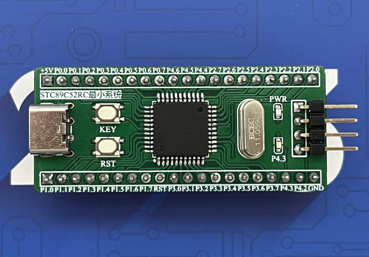
2. Onboard resources

Fig.2-1 Diagram of STC89C52RC core board resources
- Main control chip: STC89C52RC, LQFP-44;
- Power interface: TYPE C, plug-in 2Pin;
- LED: 1 power indicator, 1 status indicator;
- Buttons: 1 system reset button, 1 function button;
- Debugging interface: USB to TTL serial port burning mode, 4Pin bent pin header;
- External pins: programmable IO ports, 2 x 1×20Pin in-line pin headers;
3. Advantages and characteristics

Fig.3-1 Dimensions of the STC89C52RC core board
- The appearance of the board is small, and the size is only 53.34mm*22.86mm (2100mil*900mil);
- STC89C52RC compatible DIP-40 package for locking seats, perforated plates, and breadboards;
- Low price, ultra-low power consumption, rich function pins, high cost performance;
- Use high-quality PCB and genuine components to ensure product quality;
4. Circuit analysis

Fig.4-1 SCH_STC89C52RC minimum system
1. Power circuit
The power supply circuit is mainly composed of TYPE-C power supply circuit, using 2Pin TYPE-C interface, which is simple and convenient, easy to solder, and C1/C2 is the power filter capacitor.

Fig.4-2 TYPE-C power supply circuit
2. Main control circuit
The main control microcontroller is usedSTC89C52RC (LQFP-44 package), the working voltage is 3.3~5.5V, the working frequency range is 0~40MHz, which is equivalent to 0~80MHz of ordinary 8051, the actual working frequency can reach 48MHz, and the space size of Flash program memory is8K bytes, more than 100,000 times of erase and write, on-chip integrated 512 bytes of RAM data memory, operating temperature range of -40~85°C.

Fig.4-3 Pin definition of STC89C52RC (LQFP-44 and DIP-40)
The STC89C51RC/RD+ series is available in HD and 90C versions, which can be distinguished by the last few letters of the bottom line of text on the surface of the microcontroller.
The HD version does not have P4.4/P4.5/P4.6 ports, and there are 45~100K pull-down resistors inside the RESET pin, and the EA# pin has been pulled up to VCC.
The 90C version does not have EA and PSEN pins, and has P4.4/P4.5/P4.6 ports, and the ALE/P4.5 pins are used as ALE by defaultWhen used as a P4.5 port, you need to set it in the STC-ISP programmer when burning the user program.

Fig.4-4 Pin configuration diagram of STC89C52RC core board
Table 1-1 explains the definition and reuse of pins in the STC89C52RC core board
|
pins |
illustrate |
|
P0.0~P0.7,P1.0~P1.7 P2.0~P2.7,P3.0~P3.7 P4.2~P4.6 |
Standard I/O ports |
|
RST |
Reset the foot |
|
RXD |
Serial port 1 data receiver |
|
TXD |
Serial port 1: data transmitter |
|
T0/T1/T2 |
External input to the timer/counter |
|
T2EX |
Timer/Counter 2 Trigger control for capture/reload mode |
|
INT# |
External interrupts, falling edge interrupts, or low-level interrupts |
|
WR# |
External data memory writes pulses |
|
RD# |
External data memory reads pulses |
|
EA# |
Internal and external memory selection pins |
|
ALE |
Address latching allows signal output pins/programmed pulse input pins |
|
PSEN# |
External program memory selects signal output pins |
The capacitance here is the filtering effect, and the pins should be placed as close to the chip as possible when drawing the PCB, and the pins of the main control circuit are connected as shown in Figure 4-5.STC89C52RC.

Fig.4-5 Main control circuit STC89C52RC
The P0 port can be used as an I/O port or as an address/data multiplexing bus. The P0 port is an open-drain output, and when used for bus expansion, there is no need to add a pull resistor. When used as an I/O port, an external pull-up resistor of 4.7K~10K must be connected. Here, the P0 port pulls up two 10K rows.

Fig.4-6 Pull-up resistance at P0 port
3. Crystal oscillator circuit
The function of the crystal oscillator is to provide the clock signal to the smallest system, and the capacitance function of the crystal oscillator is to ensure that the output oscillation frequency is more stable.

Fig.4-7 crystal oscillator circuit
4. Reset circuit
Reset is also called restart, press the SW1 button, and the main control RST pin is pulled up; Release the SW1 button and the RST pin is pulled low, generating an external reset pulse to reset the system.

Fig.4-8 Reset circuit
5. Peripheral circuits
When powered on, the power indicator (red) lights up, which proves that the minimum system power supply part is working normally. The test status indicator (blue) is used to test the P4.3 pin of the MCU, and the test light is turned on and off through the program.

Fig.4-9 LED indicator circuit
Reserved a user function key, you can customize the key function, connected with the MCU P4.2, here used to test the blue light of P4.3.

Fig. 4-10 Key circuit
The USB to TTL serial port burning method is adopted, and the 1x4Pin bent socket header interface is reserved for debugging and downloading the program.

Fig.4-11 Downloading a circuit
It is convenient to expand the project, facilitate the verification of various functions, use two 1x20pin 2.54mm pin headers, lead out the I/O pins of the single-chip microcomputer, and are compatible with the pin arrangement of other mainstream single-chip microcomputer core boards.

Fig.4-12 External I/O port
5.Bill of materials
|
BOM_STC89C52RC minimal system |
||||||
|
NO. |
name |
parameter |
Device designation |
quantity |
encapsulation |
Item number |
|
1 |
resistance |
10kΩ |
R1~R3 |
3 |
R0603 |
C99198 |
|
10kΩ |
RN1,RN2 |
2 |
C107374 |
|||
|
2 |
Exclusion |
10kΩ |
RN1,RN2 |
2 |
R0603x4 |
C107374 |
|
3 |
capacitance |
10uF |
C1,C3 |
2 |
C0603 |
C85713 |
|
100nF |
C2,C4 |
2 |
C1591 |
|||
|
22pF |
C5,C6 |
2 |
C91701 |
|||
|
4 |
LED |
红灯 |
LED1 |
1 |
LED0603 |
C72044 |
|
蓝灯 |
LED2 |
1 |
C72041 |
|||
|
5 |
keystroke |
PTS815SJK250SMTRLFS |
SW1,SW2 |
2 |
KEY-SMD_4P |
C918859 |
|
6 |
Crystal oscillator |
11.0592MHz |
X1 |
1 |
HC-49US-2P |
C258977 |
|
7 |
Microcontroller |
STC89C52RC |
U1 |
1 |
LQFP-44 |
C8707 |
|
8 |
Pin header |
2.54mm 1x4P Angle insert |
H1 |
1 |
HDR-TH_4P-P2.54 |
C2935929 |
|
2.54mm 1x20P DIP |
H2,H3 |
2 |
HDR-TH_20P-P2.54 |
C429964 |
||
|
9 |
USB |
TYPE-C-2Pin |
USB1 |
1 |
TYPE-C-TH-2Pin |
C2848624 |
6. Precautions
When drawing a schematic, you should pay attention to:
- Draw according to the division of module circuits, and indicate the circuit function;
- Fill in the project name and other information on the drawing attributes;
In the purchase of materials, it should be noted that:
- Screen the in-stock materials first, and then filter the price sorting to purchase;
- Try to buy materials from the same warehouse, choose a warehouse close to it, and shorten the delivery time;
- When you purchase multiple orders, you can save shipping costs by binding orders;
In the PCB Layout, it should be noted that:
- The filter capacitor should pay attention to the current flow direction, and try to be as close as possible to the filter element;
- The crystal oscillator should be as close to the chip as possible, and the bottom should not be traced to prevent signal crosstalk;
- The line is preferentially straight, and the place that needs to be turned is mainly obtuse angle or arc;
- After the drawing is adjustedTeardrops are added after the PCB to make the board more beautiful and stable;
- Add silk screen logo and annotate interface functions;
- JLCJLCJLCJLC designated custom silk screen printing can be hidden under the device, and the board is beautiful;

Fig.6-1-1 Reference diagram of PCB traces - top layer

Fig.6-1-2 Bottom layer of PCB traces
In welding, attention should be paid to:
- When welding, you can click the welding auxiliary tool in the toolbar of Jialichuang EDA, and the real-time interaction is convenient for welding;
- When soldering the top layer, it is recommended that the main control chip be soldered first to avoid other devices affecting soldering;
- When welding the pin header, it can be used to resist an empty plate or a hole plate to prevent welding skew and affect the use;
- The welding sequence should follow the principle from low to high to avoid affecting the welding of small devices;

Fig.6-2-1 Empty PCB - top layer

Fig.6-2-2 Empty PCB - bottom layer

Fig.6-3-1 Physical view of PCBA - top surface

Fig.6-3-2 Physical PCBA diagram - bottom surface

Fig.6-4 3D rendering
During debugging, it should be noted that:
- Before power-on commissioning, check whether there are problems such as virtual welding short circuit in the welding, and check whether the test is correct.
- Use STC-ISP to download programming and burning software, the official download address: http://www.stcmcudata.com/
- Use the USB to TTL serial port burning tool to download the program to the single-chip microcomputer, and the RXD of the USB to TTL cable is terminated to the TXD end of the single-chip microcomputer. TXD terminates the RXD terminal of the microcontroller;
- After clicking Download/Programming, you need to replug and unplug the VCC to power on, and the handshake operation is successful, that is, the user code has been successfully downloaded.

Fig.6-5 STC89C52RC minimum system working diagram
Designed by 立创EDA课程案例推荐 (from OSHWHub)
Link:https://oshwhub.com/course-examples/he-xin-ban-stc89c52rc-zui-xiao-xi-tong
Design Drawing
 Empty
Empty
Comment