

 Completed
65W super GAN power charger
PRO 65W super GAN power charger
License
:GPL 3.0
Description
There was an update to the project in December 2022, which added the power supply zener diode on the secondary side of the transformer (actually measured, the secondary voltage will increase correspondingly under the 80W limit output, so this update is to prevent chip overvoltage)
A few more photos later. Bilibili video link: https://www.bilibili.com/video/BV1wr4y187bM#reply111765361936.
65W Super gan power charger supports a variety of fast charging protocols, including USB TypeC DFP, PD2.0/PD3.0/PPS, HVDCP QC4+/QC4/QC3.0/QC2.0 (Quick Charge), FCP (Hisilicon® Fast Charge Protocol), SCP (Super Fast Charge), AFC (Samsung® Adaptive Fast Charge), MTK PE+ 2.0/1.1 (MediaTek Pump Express Plus 2.0/1.1), Apple 2.4A, BC1.2 and Samsung 2.0A.
If you like my project, please like and collect it, thank you! More quality works will be released in the next issue.
Bilibili UP owner: Lei Laoba talks about electronics, QQ Q&A group 458720579.
Overall Design Plan

Schematic Design Instructions

The picture above shows the main circuit of the power supply. 220V AC enters the common mode filter and becomes 320V DC after passing through the rectifier bridge. Here we need to add an impact suppression circuit. Behind the capacitor is the main chip of the counterattack power supply SC1933C, which uses gallium nitride technology to achieve small size and high power. , the chip application is simple, practical and powerful, suitable for novices to use. This gallium nitride chip has application solutions on a variety of chargers. The price on Taobao is about five yuan per piece.

The picture above shows the secondary synchronous rectification, which uses a 100V20A NMOS tube. Q4 is the gate driver. Since there is a parasitic capacitance between the MOS tubes GS, Q4 is responsible for quickly turning off GS and improving the stability of the entire system. There is no Q4 in the actual measurement. The downstream circuit does not work and the output is in hiccup state.

The picture above shows the primary auxiliary power supply, which provides power for the gallium nitride chip SC1933. Here we should pay attention to the fact that the power supply pin of the chip must be added with a capacitor. In actual testing, it does not work without a capacitor.

The picture above shows the fast charging protocol identification chip IP2726. It supports multi-protocol fast charging without the need for external devices such as inductors. It directly controls the FB pin of the gallium nitride chip to adjust the voltage. Note that the output resistor of our gallium nitride configuration is 5V output. Do not configure it. to 20V, otherwise it will not work. IP2726_AC_FBR is a fast charging protocol IC that integrates multiple protocols and is used for USB-A and TYPE-C dual-port output. Supports multiple fast charging protocols, including USB TypeC DFP, PD2.0/PD3.0/PPS, HVDCP QC4+/QC4/QC3.0/QC2.0 (Quick Charge), FCP (Hisilicon® Fast Charge Protocol), SCP ( Super Fast Charge), AFC (Samsung® Adaptive Fast Charge), MTK PE+ 2.0/1.1 (MediaTek Pump Express Plus 2.0/1.1), Apple 2.4A, BC1.2 and Samsung 2.0A. Provide complete TYPE-C solutions for one-way output applications such as adapters and car chargers.
This chip supports port C and port A output and is available on LCSC.

The picture above shows the transformer I use. If you buy more than one, you can get free shipping.
PCB Design Instructions

The picture above shows the top layer of the PCB, which uses an isolation design to isolate low and high voltages. At the same time, the power pins of the gallium nitride chip are windowed to increase the current capability.

The picture above shows the bottom layer of the PCB. The gallium nitride chip is placed on the bottom layer, and the high-voltage part is not covered with copper.
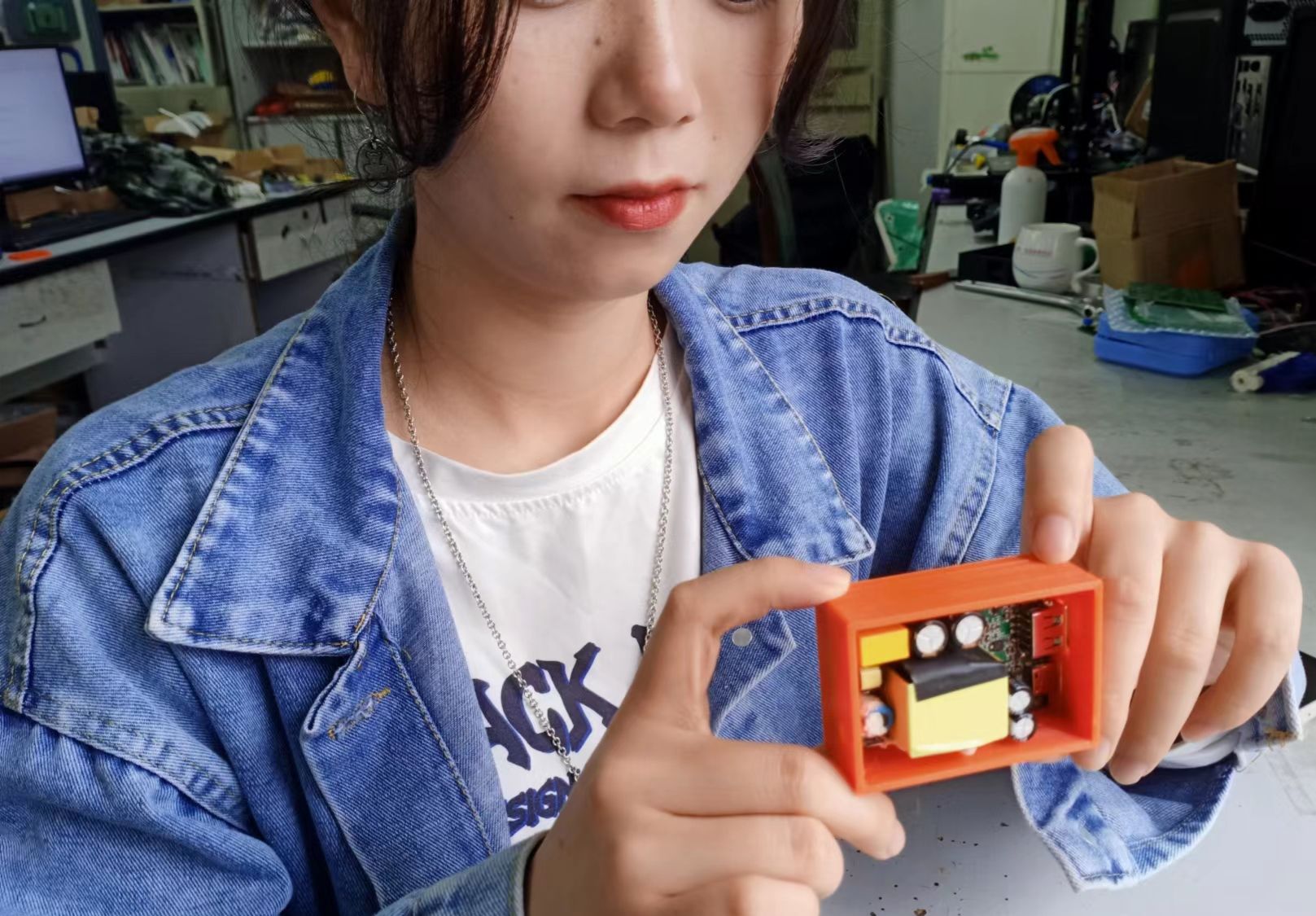
Physical Display Instructions


Announcements
Since we are using a 220V high-voltage input, we must pay attention to safety during the debugging process. If you have any questions, you can join the fan QQ group 458720579 for technical exchanges.
Demo Video Link
https://www.bilibili.com/video/BV1wr4y187bM#reply111765361936
Designed by 雷老师讲电子 (from OSHWHub)
Link:https://oshwhub.com/leichaolin/5wEcWEKPQ0yG38oIljAZBvJkkTLlbAyP
Design Drawing
 Empty
Empty
Comment